Transfer device for jet printing of film substrate, electronic printing system and electronic printing method

A technology of film substrate and transfer device, which is applied in the fields of printed circuit, printed circuit manufacturing, electrical components, etc. It can solve the problems affecting the printing efficiency and printing quality of film substrate, the accuracy of film substrate picking and feeding, and the inaccurate placement of substrate, etc. problems, to achieve the effect of saving preparation cost and application cost, improving efficiency and reducing scrap rate

Active Publication Date: 2019-12-13
武汉国创科光电装备有限公司
View PDF7 Cites 3 Cited by
  • Summary
  • Abstract
  • Description
  • Claims
  • Application Information

AI Technical Summary

Problems solved by technology

[0004] At present, most of the transfer positioning of film substrates adopts the method of manual transfer, that is, the taking and feeding of film substrates are all done manually; this method of taking and feeding materials is not only inefficient, but also has high labor costs. The accuracy of feeding is obviously affected by manual operation, and it is very easy to place inaccurate substrates, which seriously affects the printing efficiency and printing quality of film substrates, which makes the application of printed electronics technology have certain limitations.

Method used


Image

  • Transfer device for jet printing of film substrate, electronic printing system and electronic printing method
  • Transfer device for jet printing of film substrate, electronic printing system and electronic printing method
  • Transfer device for jet printing of film substrate, electronic printing system and electronic printing method

Examples


Embodiment Construction

[0047] In order to make the object, technical solution and advantages of the present invention clearer, the present invention will be further described in detail below in conjunction with the accompanying drawings and embodiments. It should be understood that the specific embodiments described here are only used to explain the present invention, not to limit the present invention.

[0048] In addition, the technical features involved in the various embodiments of the present invention described below can be combined with each other as long as they do not constitute a conflict with each other.

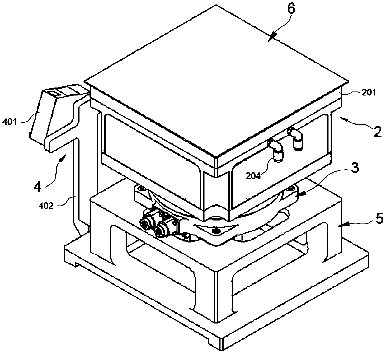
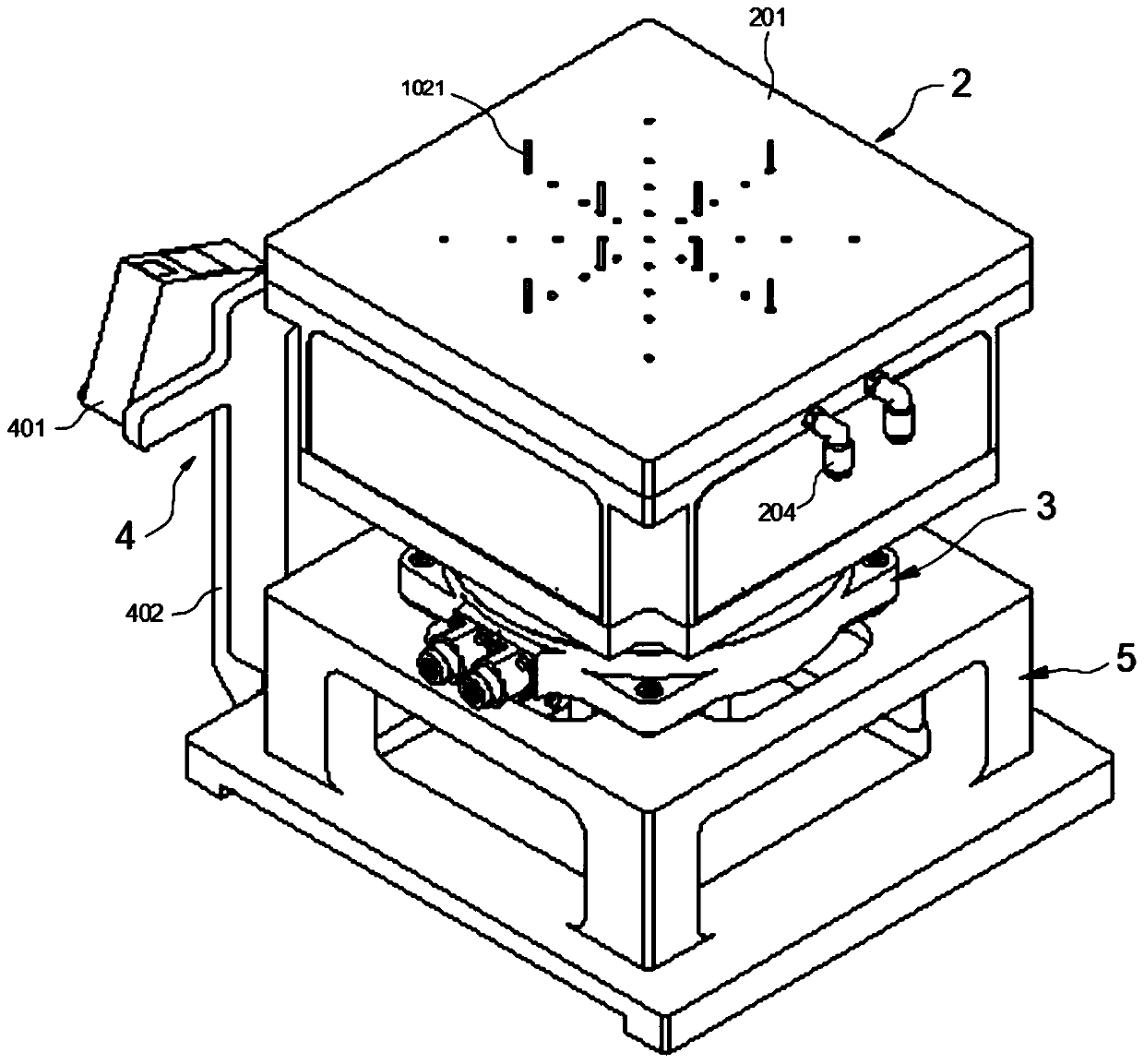
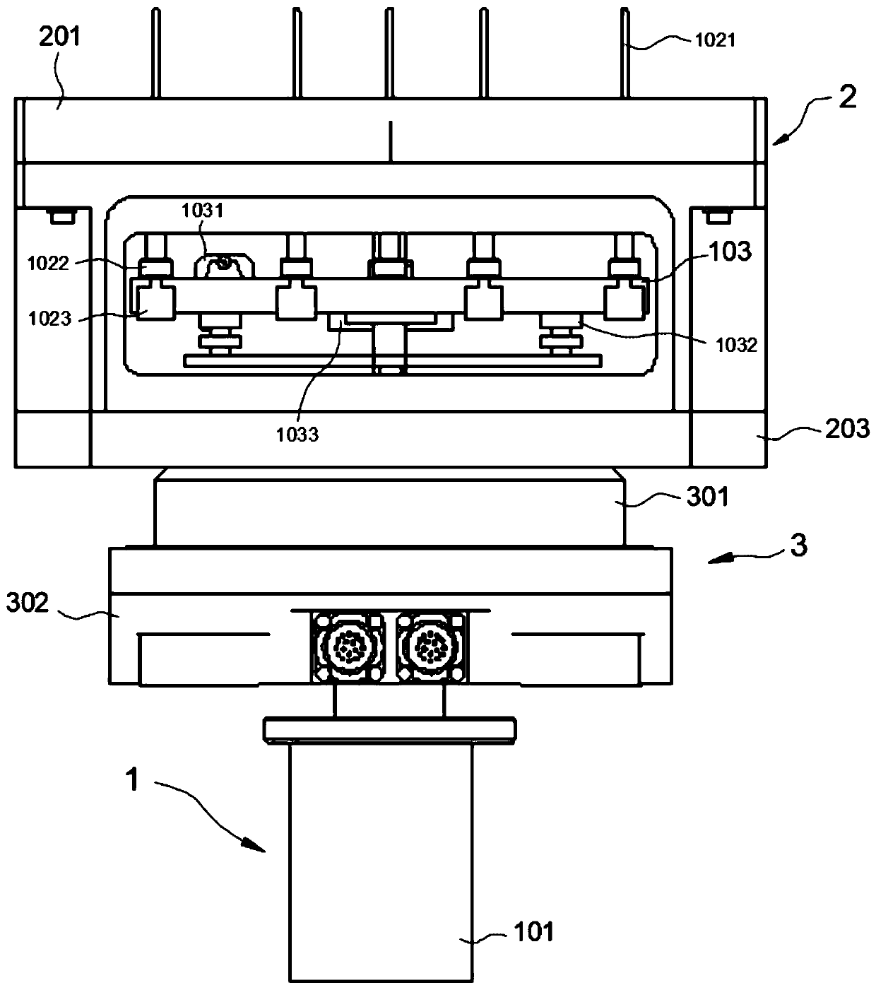
[0049] The transfer device of the jet printing thin film substrate in the preferred embodiment of the present invention is as Figure 1-7 shown in . Wherein, it includes a base 5 and an adsorption assembly 2 , a lifting assembly 1 and a rotating assembly 3 correspondingly arranged on the base 5 .

[0050] Specifically, the main body of the adsorption assembly 2 in the preferred embodi...


PUM


Abstract

The invention discloses a transfer device for jet printing of a film substrate, an electronic printing system and an electronic printing method, which belong to the technical field of printing. A lifting assembly, an adsorption assembly and a rotating assembly are correspondingly arranged on the base. The transfer device comprises a lifting motor, a support plate, a thimble mechanism, a rotating motor and the like, and by using mutual matching work of the components, stable feeding, adsorption and angle adjustment of the film substrate on the top surface of the adsorption plate can be accurately realized, and the placement accuracy of the film substrate in the electronic printing process is ensured. The transfer device for jet printing of the film substrate has the advantages that the structure is simple, the control is simple and convenient, the accuracy and the automatic degree are high, the positioning accuracy of the film substrate before printing can be greatly enhanced, the rejection rate in the preparation process of the printed circuit board is reduced, the cost is saved and the device is economical and environment-friendly. Besides, according to the electronic printing system arranged based on the transfer device, the printing method has simple steps, the control is simple and convenient, the substrate electronic printing efficiency can be further enhanced, and the substrate preparation cost is reduced.

Description

technical field [0001] The invention belongs to the technical field of printed electronics, and in particular relates to a transfer device for spray printing a film substrate, an electronic printing system including the transfer device, and a method for electronically printing a film substrate by using the electronic printing system. Background technique [0002] Printed electronics technology is a technology that prints circuits on plastic films or glass substrates. It is a green manufacturing technology that has the advantages of less material, low cost, no pollution, and high flexibility. It greatly simplifies the manufacturing process of electronic products and prepares Various types of products, such as ultra-thin, bendable, small or large or light-weight products. By using the screen printing or roller printing technology that has matured in the printing industry, using suitable substrates and conductive "inks", circuit boards can be printed in large quantities. [00...

Claims


Application Information

Patent Timeline
Patent Type & Authority Applications(China)
IPC IPC(8): H05K3/00H05K3/12B65G47/91
CPCB65G47/914B65G2201/022H05K3/0008H05K3/12
Inventor 尹周平陈建魁高俊伟雷春耀
Owner 武汉国创科光电装备有限公司
Why Eureka
Try Eureka