Trench MOSFET integrated with ESD protection and manufacturing method thereof

An ESD protection and manufacturing method technology, applied in semiconductor/solid-state device manufacturing, electrical components, diodes, etc., can solve the problems of increasing the clamping voltage and impedance of the energy discharge channel, increasing the difficulty of the process, and poor process stability, achieving The effect of stable ESD discharge characteristics, stable ESD protection ability and good ESD protection ability

Pending Publication Date: 2019-11-29
深圳市芯电元科技有限公司
View PDF1 Cites 0 Cited by
  • Summary
  • Abstract
  • Description
  • Claims
  • Application Information

AI Technical Summary

Problems solved by technology

[0007] 1. In order to make thick oxide layer and polysilicon diode, the process flow is more complicated and the process cost is higher
[0008] 2. Due to the thick oxide layer and polysilicon diodes, the step difference on the chip surface is relatively large, which increases the difficulty of the process and poor process stability
[0009] 3. The Zener diode uses polysilicon diodes, and polysilicon is composed of silicon grains of a certain size. Its stability and consistency are worse than those of single crystal silicon. Therefore, Zener diodes made of polysilicon have better ESD protection capabilities. The stability is also poor
[0010] 4. The Zener diode is located between the gate and the source, not between the gate and the drain, so the ESD energy between the gate and the drain can only pass through the Zener diode and the body of the MOSFET The series loop composed of parasitic diodes discharges, that is, the ESD energy discharge channel between the gate and the drain has one more internal parasitic diode than the ESD energy discharge channel between the gate and the source, thereby increasing the energy discharge The clamping voltage and impedance of the channel, therefore, typically results in less ESD protection between gate and drain than between gate and source

Method used


Image

  • Trench MOSFET integrated with ESD protection and manufacturing method thereof
  • Trench MOSFET integrated with ESD protection and manufacturing method thereof
  • Trench MOSFET integrated with ESD protection and manufacturing method thereof

Examples


Embodiment 1

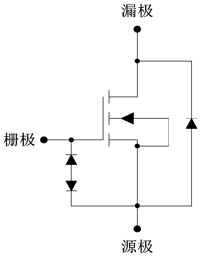
[0080] Embodiment 1: A trench MOSFET with integrated ESD protection, see figure 2 , image 3 .

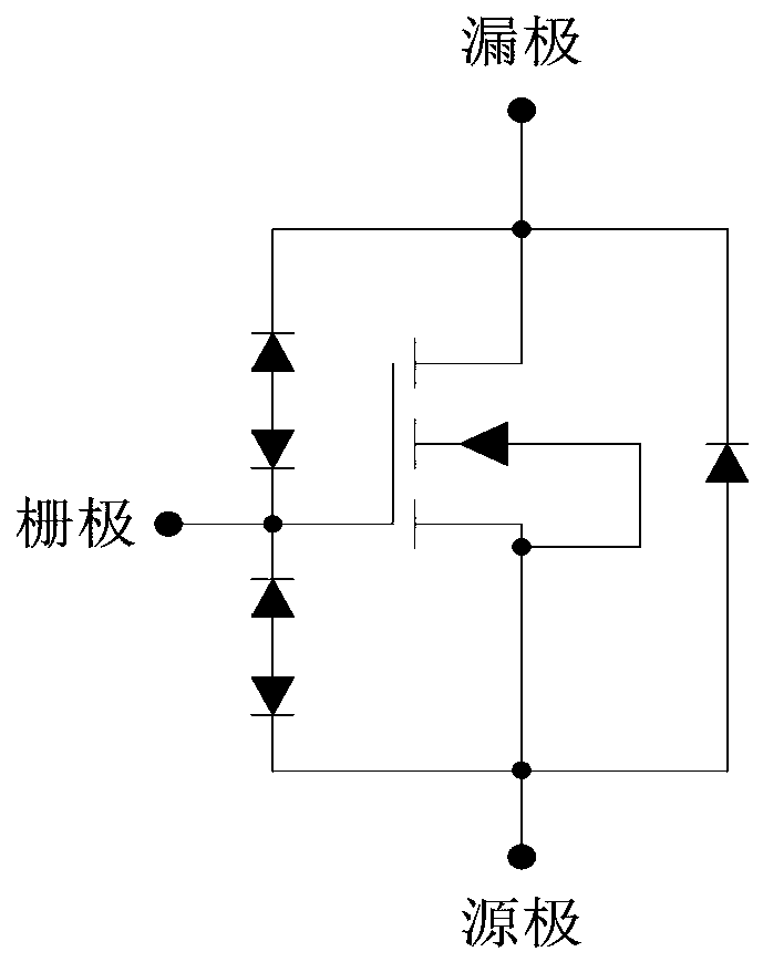
[0081] The trench MOSFET of integrated ESD protection of the present invention, can refer to figure 2 Between the gate and the source of the MOSFET, there is a Zener diode composed of forward and reverse PN junctions connected in series, one end of the Zener diode is connected to the gate of the MOSFET, and the other end is connected to the source of the MOSFET; Between the gate and the drain of the gate, there is a Zener diode composed of forward and reverse PN junctions connected in series, one end of the Zener diode is connected to the gate of the MOSFET, and the other end is connected to the drain of the MOSFET; the Zener diode Both are body silicon diodes, and their equivalent circuit diagrams are shown in image 3 shown.

[0082] Such as figure 2 As shown, the Zener diode is located under the gate of the MOSFET and the surrounding area of ​​the gate. Between the Zener...

Embodiment 2

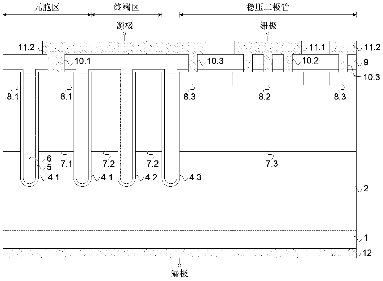
[0095] Example 2, see Figure 4 to Figure 12 , a method for manufacturing a trench MOSFET with integrated ESD protection, which is used to manufacture the trench MOSFET with integrated ESD protection described in Example 1, and the trench MOSFET with integrated ESD protection described in Example 1 is suitable for N Type trench MOSFET and P-type trench MOSFET, for ease of understanding and description, this embodiment takes the manufacturing method of N-type trench MOSFET as an example for illustration, specifically it includes the following steps:

[0096] S1. Form a lightly doped N-type epitaxial layer 2 on the upper surface of a heavily doped N-type silicon substrate 1, see Figure 4 .

[0097] S2, forming a hard mask 3 on the upper surface of the N-type epitaxial layer 2, the material of the hard mask 3 is silicon oxide or silicon nitride, or a stacked layer formed of silicon oxide and silicon nitride, the hard mask 3 has a thickness of 200-600nm, see Figure 5 .

[00...


PUM

PropertyMeasurementUnit
Thicknessaaaaaaaaaa
Thicknessaaaaaaaaaa

Abstract

The invention discloses a more excellent trench MOSFET integrated with ESD protection and a manufacturing method thereof. The trench MOSFET integrated with ESD protection comprises a voltage stabilizing diode formed by connecting a positive PN junction and a negative PN junction in series between a grid electrode and a source electrode of the MOSFET, wherein one end of the voltage stabilizing diode is connected with the grid electrode of the MOSFET, and the other end of the voltage stabilizing diode is connected with the source electrode of the MOSFET. The trench MOSFET integrated with ESD protection comprises a voltage stabilizing diode formed by connecting a positive PN junction and a negative PN junction in series between the grid electrode and a drain electrode of the MOSFET, wherein one end of the voltage stabilizing diode is connected with the grid electrode of the MOSFET, and the other end of the voltage stabilizing diode is connected with the drain electrode of the MOSFET. In the manufacturing method of the trench MOSFET integrated with ESD protection, a P-type doped region of the voltage stabilizing diode integrated in the trench MOSFET and a P-type body region of the MOSFET can be synchronously formed in process, and an N-type doped region of the voltage stabilizing diode and an N-type source region of the MOSFET can be synchronously formed in process, so that lower manufacturing cost is realized.

Description

technical field [0001] The invention relates to the technical field of semiconductor device manufacturing, in particular to a trench MOSFET with integrated ESD protection and a manufacturing method. Background technique [0002] MOSFET chips are classified according to structure, including planar MOSFET and trench MOSFET. Among them, trench MOSFET occupies a dominant position in medium and low voltage MOSFETs due to its higher current density; MOSFET chips are classified according to conduction methods, including N-type MOSFET and P-type MOSFETs, where N-type MOSFETs are more widely used due to their higher current density. MOSFET chips include three ports: source, gate, and drain. Usually, the source and gate are on the front of the chip, and the drain is on the back of the chip. [0003] There is a thin gate oxide layer between the gate and the source and drain of the MOSFET chip, which will be damaged by breakdown and cannot be recovered when it is subjected to an unexpe...

Claims


Application Information

Patent Timeline
IPC IPC(8): H01L29/06H01L27/02H01L29/78H01L21/336
CPCH01L29/0603H01L27/0255H01L29/78H01L29/66477
Inventor 潘光燃
Owner 深圳市芯电元科技有限公司
Why Eureka
Try Eureka