Manufacturing method for conductive film based on printing process
A manufacturing method and technology of conductive film, which can be applied to equipment for manufacturing conductive/semiconductive layer, conductive layer on insulating carrier, cable/conductor manufacturing, etc. Problems such as uneven thickness, to avoid the coffee ring effect and increase the surface wettability
- Summary
- Abstract
- Description
- Claims
- Application Information
AI Technical Summary
Problems solved by technology
Method used
Image

Examples
Embodiment 1
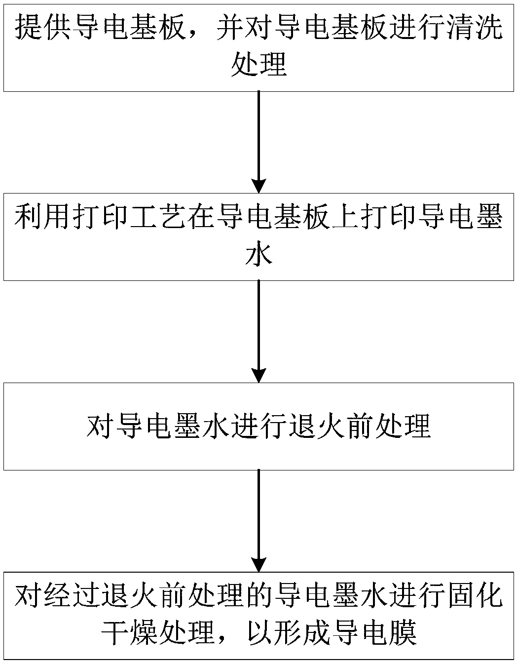
[0041] Figure 2A to Figure 2E A process diagram of a conductive film according to Embodiment 1 of the present invention is shown. The method for manufacturing a conductive film based on a printing process includes steps S01 to S04:
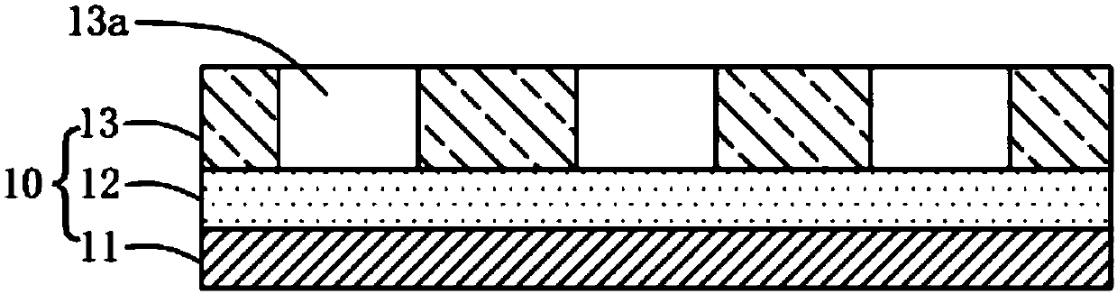
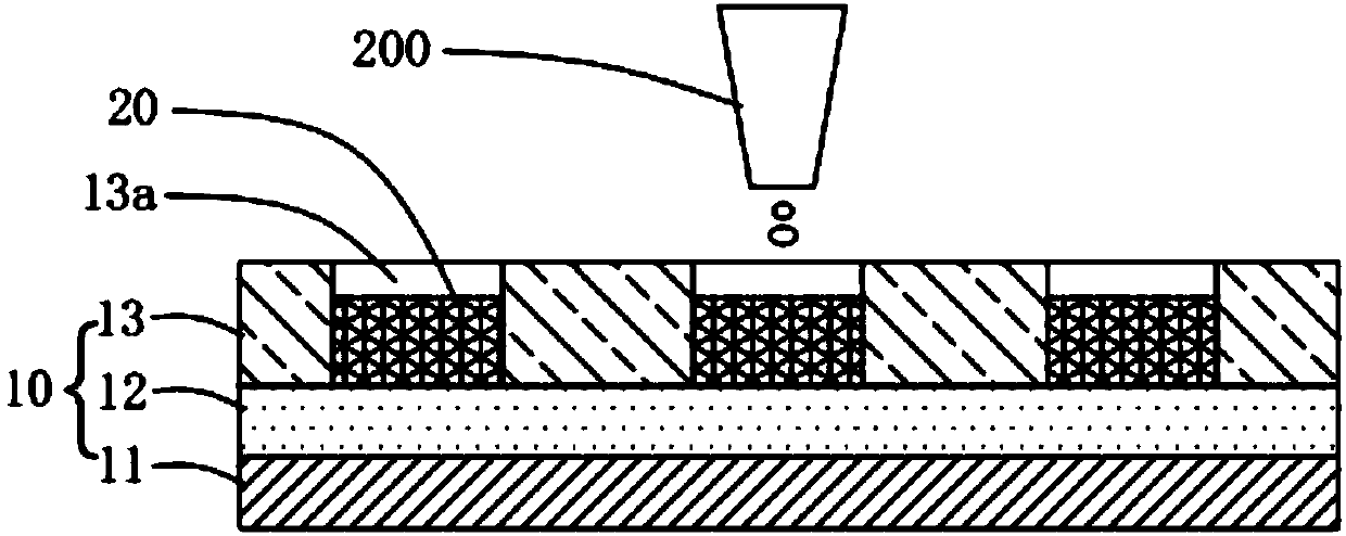
[0042] Specifically, step S01: as Figure 2A As shown, a conductive substrate 10 is provided, and the conductive substrate 10 is cleaned. As a preferred embodiment, the conductive substrate 10 includes a substrate 11, a conductive layer 12 disposed on the substrate 11, and a pixel defining layer disposed on the conductive layer 12 13. The substrate 11 is preferably a glass substrate, and the pixel defining layer 13 includes a plurality of through holes 13a arranged at intervals, and the through holes 13a and the conductive layer 12 enclose pixel pits. The material of the conductive layer 12 is preferably a transparent electrode material, such as ITO. As a preferred embodiment, the shape of the through hole 13a is elliptical, the major axis of t...
Embodiment 2
[0051] The method for manufacturing a conductive film based on a printing process according to Embodiment 2 of the present invention includes steps S11 to S14:
[0052] Step S11: providing a conductive substrate 10, and cleaning the conductive substrate 10. The structure of the conductive substrate 10 in the second embodiment includes a substrate 11, a conductive layer 12 disposed on the substrate 11, and a pixel defining layer 13 disposed on the conductive layer 12. The substrate 11 is preferably a flexible substrate, and the material of the flexible substrate is poly Ethylene terephthalate, the conductive layer 12 and the pixel defining layer 13 in this embodiment are the same as those in the first embodiment, and will not be repeated here. The method of cleaning the conductive substrate 10 in the second embodiment is the same as the method of cleaning the conductive substrate 10 in the first embodiment, and will not be repeated here.
[0053] Step S12: Print the conductive...
Embodiment 3
[0059] The method for manufacturing a conductive film based on a printing process according to Embodiment 2 of the present invention includes steps S21 to S24:
[0060] Specifically, step S21: as Figure 4A As shown, a conductive substrate 10 is provided, and the conductive substrate 10 is cleaned. As a preferred embodiment, the conductive substrate 10 includes a substrate 11 and a conductive layer 12 disposed on the substrate 11, the substrate 11 is preferably a glass substrate, and the material of the conductive layer 12 is preferably a transparent electrode material, such as ITO. The method of cleaning the conductive substrate 10 in the third embodiment is the same as the method of cleaning the conductive substrate 10 in the first embodiment, and will not be repeated here.
[0061] Step S22: if Figure 4B As shown, the conductive ink 20 is printed on the conductive substrate 10 using an inkjet printing process. Specifically, the conductive ink 20 in this embodiment inclu...
PUM
| Property | Measurement | Unit |
|---|---|---|
| Viscosity | aaaaa | aaaaa |
| Surface tension | aaaaa | aaaaa |
| Viscosity | aaaaa | aaaaa |
Abstract
Description
Claims
Application Information
 - R&D
- Intellectual Property
- Life Sciences
- Materials
- Tech Scout
- Unparalleled Data Quality
- Higher Quality Content
- 60% Fewer Hallucinations
Browse by: Latest US Patents, China's latest patents, Technical Efficacy Thesaurus, Application Domain, Technology Topic, Popular Technical Reports.
© 2025 PatSnap. All rights reserved.Legal|Privacy policy|Modern Slavery Act Transparency Statement|Sitemap|About US| Contact US: help@patsnap.com