Electrochemical imaging system and method based on graphene adjustable light scattering property
An imaging system, graphene technology, applied in the direction of scattering characteristics measurement, material electrochemical variables, methods of obtaining spatial resolution, etc., can solve problems such as failure to break through, and achieve the effect of function and performance improvement
- Summary
- Abstract
- Description
- Claims
- Application Information
AI Technical Summary
Problems solved by technology
Method used
Image
Examples
Embodiment 1
[0046] Such as figure 1 , an electrochemical imaging system based on the tunable light scattering properties of graphene, including a graphene electrolytic cell system 1, a microscope system 2, an imaging module 3 and an image processing module 4;
[0047] The graphene electrolytic cell system 1 includes a working electrode 11, a counter electrode 12, a reference electrode 13 and an electrolytic solution 14, and the working electrode 11 is graphene; specifically, the graphene used in this embodiment is a single layer or Few layers (3-5 layers) of graphene grown by CVD, platinum wire as counter electrode, silver / silver chloride as reference electrode, and electrolyte solution as potassium nitrate solution; wherein, graphene electrode can be obtained by other methods, such as evaporation Plating, transfer, growth, etc.; the counter electrode and reference electrode can be replaced by other conductive materials.
[0048] Described graphene electrolytic cell system 1 links to eac...
Embodiment 2
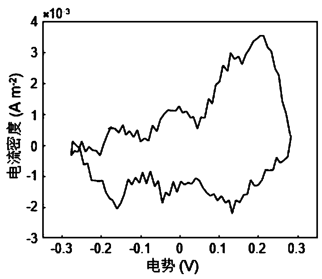
[0058] Using the electrochemical imaging system based on the adjustable light scattering properties of graphene described in Example 1, the electrochemical workstation is used to apply a triangular wave potential with a scan rate of 0.1V / s and a range of -0.3 to 0.3V to the working electrode for cyclic voltammetry scanning.
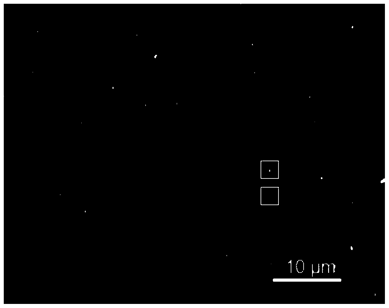
[0059] Such as image 3 , the image processing module extracts the picture obtained by the imaging module, and obtains the current density of a single gold nanostar by performing calculation processing on the scattered light intensity of the picture;
[0060]
[0061] As shown in the figure, the noise of calculating the current density by the standard deviation is 7.18×10 -4 Am -2 . The near-field scattering cross section of the gold nanostar is 2.10×10 -15 m 2 . Therefore, by calculating the three times the signal-to-noise ratio of the current noise, the detection limit of the current is 4.52 × 10 -18 A, that is 4.52aA.
[0062] Based on the a...
Embodiment 3
[0064] Same as Example 2, the difference is that 1mM potassium ferricyanide is added to the electrolyte, and a triangular wave potential with a sweep rate of 0.1V / s and a range of -0.6 to 0.6V is applied to the working electrode to perform cyclic voltammetry scanning.
[0065] The image processing module extracts the picture obtained by the imaging module, and calculates the scattered light intensity of the picture through the following formula to obtain the local current density representing the target sample, and realize the imaging analysis of the electrochemical reaction on a single nanostar;
[0066]
[0067] At the same time, the macroscopic cyclic voltammetry curve collected by the graphene electrolytic cell system.
[0068] Such as Figure 4 a-d, when the potential is -0.6V, there is no obvious current on the surface of the gold nanostar. When the potential is swept to 0.12V, there is the largest oxidation current, and then gradually disappears, and the reduction cu...
PUM
 Abstract
Description
Claims
Application Information
 - R&D
- Intellectual Property
- Life Sciences
- Materials
- Tech Scout
- Unparalleled Data Quality
- Higher Quality Content
- 60% Fewer Hallucinations
Browse by: Latest US Patents, China's latest patents, Technical Efficacy Thesaurus, Application Domain, Technology Topic, Popular Technical Reports.
© 2025 PatSnap. All rights reserved.Legal|Privacy policy|Modern Slavery Act Transparency Statement|Sitemap|About US| Contact US: help@patsnap.com


