Quantum dot photoelectric detector and preparation method

A photodetector, quantum dot technology, applied in photovoltaic power generation, electric solid state device, semiconductor/solid state device manufacturing, etc., can solve the problem of large dark current of quantum dot photodetector, reduce dark current and enhance photoelectric performance Effect

Pending Publication Date: 2019-10-22
SOUTH UNIVERSITY OF SCIENCE AND TECHNOLOGY OF CHINA
View PDF5 Cites 0 Cited by
  • Summary
  • Abstract
  • Description
  • Claims
  • Application Information

AI Technical Summary

Problems solved by technology

[0005] In view of this, an embodiment of the present invention provides a quantum dot photodetector and a preparation method to solve the technical problem that the quantum dot photodetector has a large dark current during operation in the prior art

Method used


Image

  • Quantum dot photoelectric detector and preparation method
  • Quantum dot photoelectric detector and preparation method
  • Quantum dot photoelectric detector and preparation method

Examples


Embodiment 1

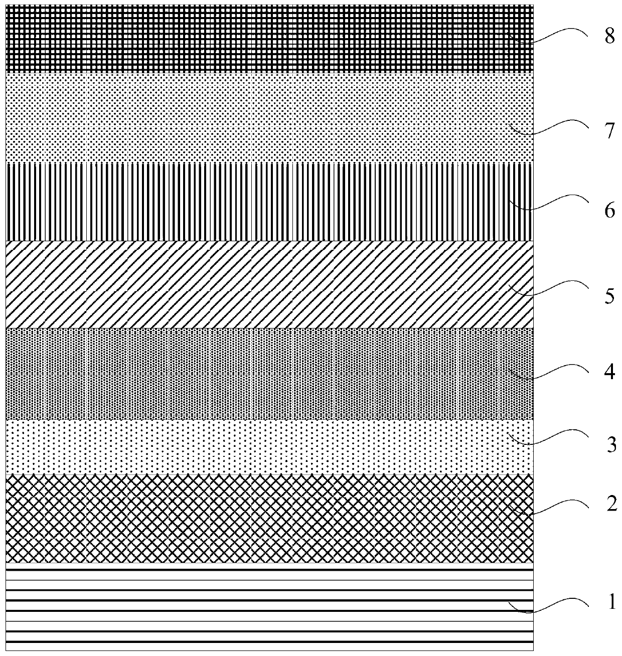
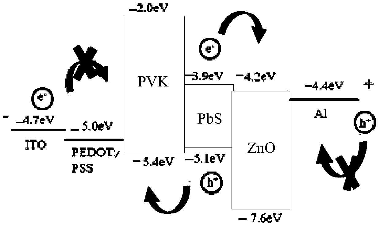
[0042] The embodiment of the present invention provides a schematic structural diagram of a quantum dot photodetector, as figure 1 As shown, the quantum dot photodetector comprises: a substrate 1; an anode 2 formed on the substrate 1; a hole transport layer 3 formed on the anode 2; an electron blocking layer 4 formed on the hole transport layer 3; The quantum dot active layer 5 on the electron blocking layer 4; the hole blocking layer 6 formed on the quantum dot active layer 5; the electron transport layer 7 formed on the hole blocking layer 6; the electron transport layer 7 formed on on the cathode 8.

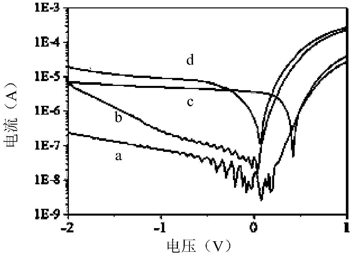
[0043] In this embodiment, the role of the quantum dot photodetector is to convert optical signals into electrical signals, which is equivalent to a converter of energy signals. Wherein, the quantum dot active layer 5 generates photogenerated carriers under the irradiation of light, the anode 2 of the quantum dot photodetector applies a negative voltage, and the cathode 8 app...

Embodiment 2

[0058] On the basis of the above-mentioned embodiments, the embodiments of the present invention provide a method for preparing a quantum dot photodetector to figure 1 The structural schematic diagram of the quantum dot photodetector shown is taken as an example for illustration, and the preparation method of the quantum dot photodetector can be found in Figure 5 , including the following steps:

[0059] Step 110, providing a substrate.

[0060] see figure 1 , providing base 1.

[0061] Step 120, forming an anode on the substrate.

[0062] see figure 1 , forming an anode 2 on a substrate 1 .

[0063] Step 130, forming a hole transport layer on the anode.

[0064] see figure 1 , forming a hole transport layer 3 on the anode 2 .

[0065] Step 140, forming an electron blocking layer on the hole transport layer.

[0066] see figure 1 , forming an electron blocking layer 4 on the hole transport layer 3 .

[0067] Step 150, forming a quantum dot active layer on the elect...


PUM


Abstract

The embodiment of the invention discloses a quantum dot photoelectric detector and a preparation method. The quantum dot photoelectric detector comprises a substrate; an anode formed on the substrate;a hole transport layer formed on the anode; an electron blocking layer formed on the hole transport layer; a quantum dot active layer formed on the electron blocking layer; a hole blocking layer formed on the quantum dot active layer; an electron transport layer formed on the hole blocking layer; and a cathode formed on the electron transport layer. According to the technical scheme provided by the embodiment of the invention, injection holes of the cathode are prevented from being transmitted from the cathode to the quantum dot active layer through the hole blocking layer, injection electrons of the anode are prevented from being transmitted from the anode to the quantum dot active layer through the electron blocking layer, dark current is reduced, and thus the photoelectric performanceof the photoelectric detector is enhanced.

Description

technical field [0001] The embodiments of the present invention relate to the technical field of electronic display, in particular to a quantum dot photodetector and a preparation method. Background technique [0002] Photodetectors are currently important optoelectronic components in the optoelectronic information industry, and are often used in sensing, detection and imaging. At present, traditional photodetector materials such as Si, Ge, and InGaAs have disadvantages such as complex preparation process, high cost, and non-flexibility. Researchers have begun to use quantum dot materials to prepare high-performance photodetectors, and their performance can exceed the current market. An order of magnitude higher than conventional photodetectors. [0003] Quantum dot is a new type of nano-optoelectronic material. Since its particle size is several to tens of nanometers, which is smaller than the Bohr radius of the material itself, electrons will be subject to three-dimension...

Claims


Application Information

Patent Timeline
Patent Type & Authority Applications(China)
IPC IPC(8): H01L51/42H01L51/48
CPCH10K30/10Y02E10/549
Inventor 王恺李晨昊孙小卫郑凡凯刘皓宸
Owner SOUTH UNIVERSITY OF SCIENCE AND TECHNOLOGY OF CHINA
Why Eureka
Try Eureka