


Quick Research
Generate reliable direction feasibility study reports for your R&D in just a few steps.

Technical Q&A
Discover and master advanced knowledge NOW. Basics, ideas, possibilities, all at once.

Find Solutions
As an expert in R&D theories, this can generate solutions to your technical problems instantly.

Evaluate Feasibility
Analyze your overall solution with one click, know your potential R&D risks in advance.

Monitor Landscape
Get weekly tech updates, stay abreast of the latest tech innovations and key insights.
Electromagnetic wave shield film, and shielded printed wiring board equipped with same
A technology for printed wiring boards and shielding films, applied in the fields of magnetic field/electric field shielding, crosstalk/noise/electromagnetic interference reduction (, printed circuits, etc.), which can solve problems such as the difficulty of thinning electromagnetic wave shielding films, and achieve excellent shielding properties.
- Summary
- Abstract
- Description
- Claims
- Application Information
AI Technical Summary
Problems solved by technology
Method used
Image

Examples
Embodiment 1)
[0084]
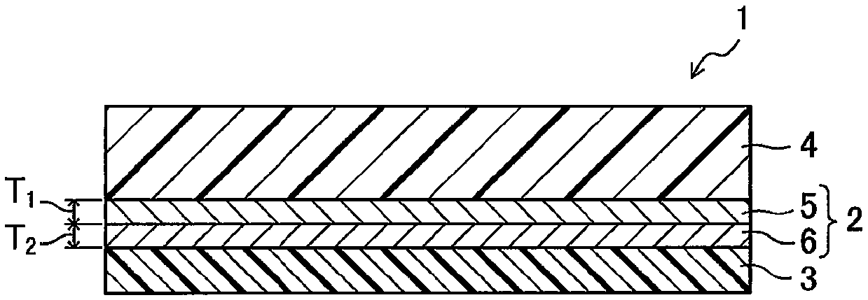
[0085] As a supporting base material, a PET film having a thickness of 60 μm and having a release treatment on the surface was used. Next, a composition for a protective layer (solid content: 30% by mass) composed of bisphenol novolac A-type epoxy resin (manufactured by Mitsubishi Chemical Co., Ltd., jER1256) and methyl ethyl ketone was applied on the supporting substrate, and By heating and drying, a support substrate with a protective layer having a thickness of 5 μm was produced.
[0086] Next, a shielding layer was formed on the surface of the protective layer. More specifically, a support substrate with a protective layer was installed in a batch vacuum evaporation apparatus (EBH−800 manufactured by ULVAC), and the vacuum arrival degree was adjusted to 5×10 in an argon atmosphere. −1 Below Pa, nickel was vapor-deposited to a thickness of 4.0 μm by a magnetron sputtering method (DC power supply output: 3.0 kW), and a first metal layer was formed.
[0087] Next...
Embodiment 2)
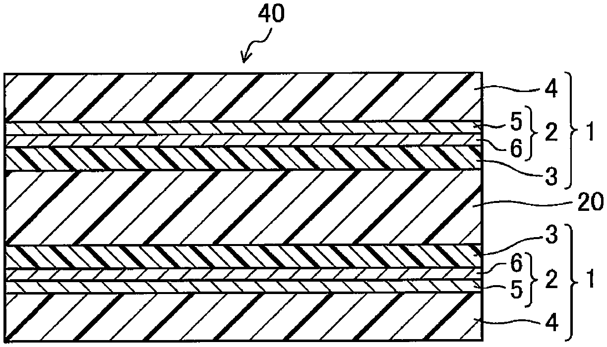
[0106] Except that the thickness of the first metal layer made of nickel was changed to 2 μm, an electromagnetic wave shielding film and a shielded printed wiring board were produced in the same manner as in Example 1, and the electric field wave and magnetic field wave shielding characteristics and output waveform characteristics were evaluated. Image 6 , Figure 7 , Figure 9 The above results are shown in .
PUM
 Abstract
Description
Claims
Application Information
 - R&D Engineer
- R&D Manager
- IP Professional
- Industry Leading Data Capabilities
- Powerful AI technology
- Patent DNA Extraction
Browse by: Latest US Patents, China's latest patents, Technical Efficacy Thesaurus, Application Domain, Technology Topic, Popular Technical Reports.
© 2024 PatSnap. All rights reserved.Legal|Privacy policy|Modern Slavery Act Transparency Statement|Sitemap|About US| Contact US: help@patsnap.com