An aberration-eliminating liquid-dielectric metalens

A technology of liquid medium and metalens, applied in lenses, instruments, optics, etc., can solve problems such as flattening a single metalens, inability to overcome imaging difficulties, large high-order aberrations, etc., to avoid abnormal spatial arrangement , Eliminate technical bottlenecks, eliminate the effect of high-order aberrations

Active Publication Date: 2020-05-12
UNIV OF ELECTRONICS SCI & TECH OF CHINA
View PDF5 Cites 0 Cited by
  • Summary
  • Abstract
  • Description
  • Claims
  • Application Information

AI Technical Summary

Problems solved by technology

In the specific design process of the metalens, the symmetrical structure of the array unit can be reasonably designed for the parallel light on the axis, and the wavefront phase of the outgoing light is constructed to be spherical, but it cannot overcome the coma aberration (produced by off-axis light source) and astigmatism (large Imaging difficulties caused by high-order aberrations such as meridional and sagittal deviations caused by the field of view), distortion (image scale imbalance caused by a large field of view)
The inability to control the wavefront phase in real time to meet the focusing requirements, or the large high-order aberrations caused by the symmetry of the array structure, is the technical bottleneck that plagues the planar single metalens to achieve a more perfect imaging effect

Method used


Image

  • An aberration-eliminating liquid-dielectric metalens
  • An aberration-eliminating liquid-dielectric metalens
  • An aberration-eliminating liquid-dielectric metalens

Examples


Embodiment Construction

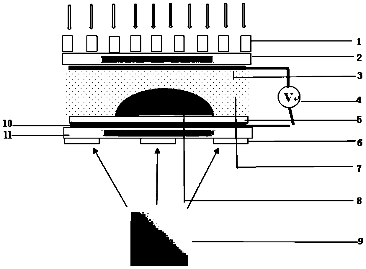
[0030] The present invention will be further described below in conjunction with the accompanying drawings and specific embodiments. Taking the elimination of the aberration produced by the traditional single-layer symmetric metalens as an example, an aberration-eliminating liquid medium metalens is implemented as follows.

[0031] Such as figure 1 As shown, an aberration-eliminating liquid medium metalens includes an upper layer metasurface array, an upper layer metalens quartz substrate, a polymer layer, a lower layer metalens quartz substrate, and a lower layer metasurface array arranged in sequence from top to bottom.

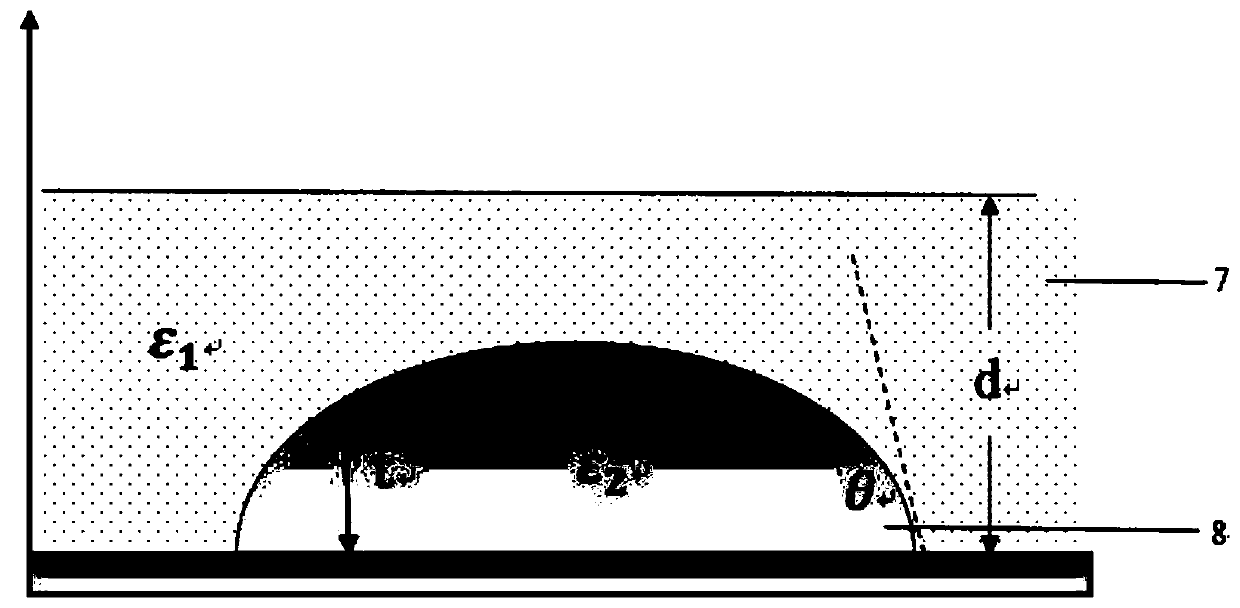
[0032] The upper and lower metasurface arrays are respectively located on both sides of the core gap layer, and are attached to the upper and lower metalens quartz substrates. The upper and lower superlens quartz substrates are coated with a layer of ITO conductive thin film (indium tin oxide, indium tin oxide layer) on the side close to the core gap layer...


PUM


Abstract

The invention discloses an aberration-eliminating liquid medium superlens, which belongs to the field of micro-nano optical imaging. The superlens includes: an upper metasurface array arranged in sequence from top to bottom, an upper superlens quartz substrate with an ITO conductive layer coated on the lower surface, a polymer layer, and a lower superlens quartz substrate with an ITO conductive layer coated on the upper surface 1. The lower metasurface array; the high molecular polymer layer is attached with a low dielectric constant liquid medium, and the high molecular polymer layer and the upper super lens quartz substrate are filled with a high dielectric constant liquid medium. The upper metasurface array of the present invention adjusts the incident light wavefront, fills the gap between two liquid media to form spherical waves required for focusing, and then the lower metasurface array eliminates the influence of interference waves and outputs focused transmitted light. Through the change of the applied voltage, the wavefront phase of the transmitted wave is finally controlled to make up for the original deficiency of the metasurface and achieve the effect of aberration elimination. A metalens optical system with wide application prospects and value is constructed.

Description

technical field [0001] The invention belongs to the field of micro-nano optical imaging, and in particular relates to a technical method for eliminating aberrations by combining a super-lens with a liquid medium. Background technique [0002] Because the metalens has many advantages such as thinness and easy adjustment, it will greatly optimize various indicators when it is used for imaging, such as reducing the quality of the optical system, expanding the range of focal length adjustment, improving the repeatability of lens design, and planarization and light weight. level increase, etc. And because of its singular characteristics based on the generalized Snell law of catadioptric reflection, it is easy to reasonably control the wavefront phase, so that it can obtain better performance than existing lenses. It is a popular choice for the design, manufacture and production of optical lenses in the future. [0003] Before an optical system is put into formal use, it is often...

Claims


Application Information

Patent Timeline
Patent Type & Authority Patents(China)
IPC IPC(8): G02B26/00G02B1/00G02B3/12
CPCG02B1/002G02B3/12G02B26/005
Inventor 李瑞峰刘涵付永启
Owner UNIV OF ELECTRONICS SCI & TECH OF CHINA
Why Eureka
Try Eureka