Overcurrent correction method and circuit of tia used in optical receiver

An optical receiver and overload current technology, which is applied in the field of optical communication, can solve problems such as increased power consumption and complex circuit design, and achieve the effects of reducing components, keeping bandwidth unchanged, and reducing parasitic capacitance

Active Publication Date: 2021-06-29
成都英思嘉半导体技术有限公司
View PDF5 Cites 0 Cited by
  • Summary
  • Abstract
  • Description
  • Claims
  • Application Information

AI Technical Summary

Problems solved by technology

However, in differential TIA circuits such as Figure 4 shown) and pseudo-differential TIA circuits (such as Figure 5 In the structure shown), due to the increase of devices, if the above method is directly used to prevent input current overload, it will cause problems such as complicated circuit design and increased power consumption.

Method used


Image

  • Overcurrent correction method and circuit of tia used in optical receiver
  • Overcurrent correction method and circuit of tia used in optical receiver
  • Overcurrent correction method and circuit of tia used in optical receiver

Examples


Embodiment 1

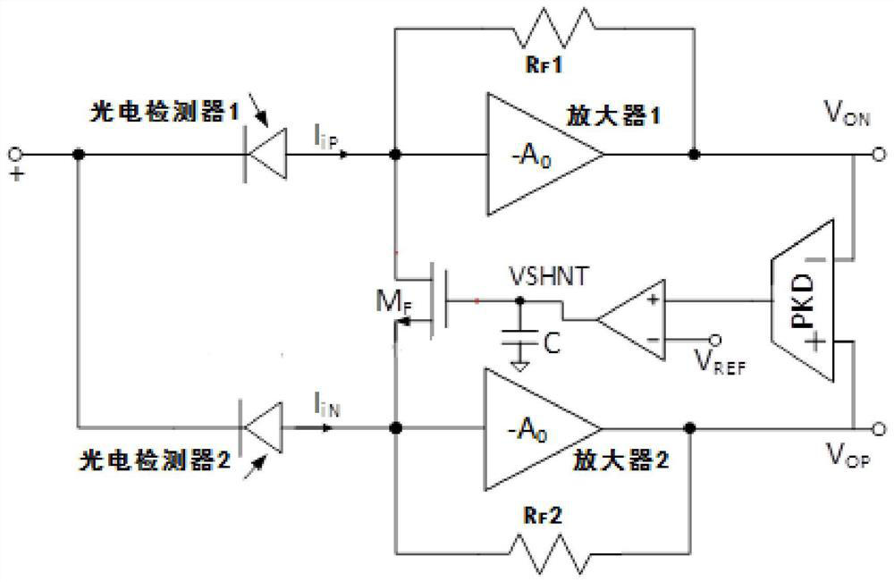
[0041] The steps of an overload current correction method for a 100-600G optical receiver transimpedance amplifier include:

[0042] The voltage values ​​of the two output terminals of the pseudo-differential transimpedance amplifier circuit are respectively collected through the differential peak detector, and the output voltage values ​​of the two channels are positive voltage signals and negative voltage signals respectively.

[0043] The differential peak detector saves the positive peak value of the positive voltage signal and the negative peak value of the negative voltage signal, and makes a difference between the positive peak value and the negative peak value, and outputs the peak differential parameter;

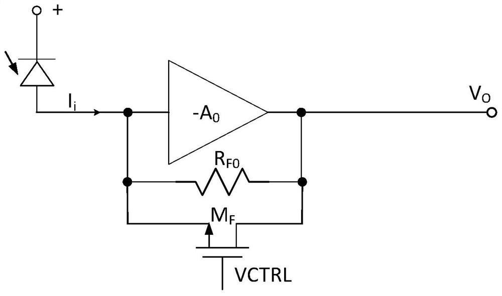
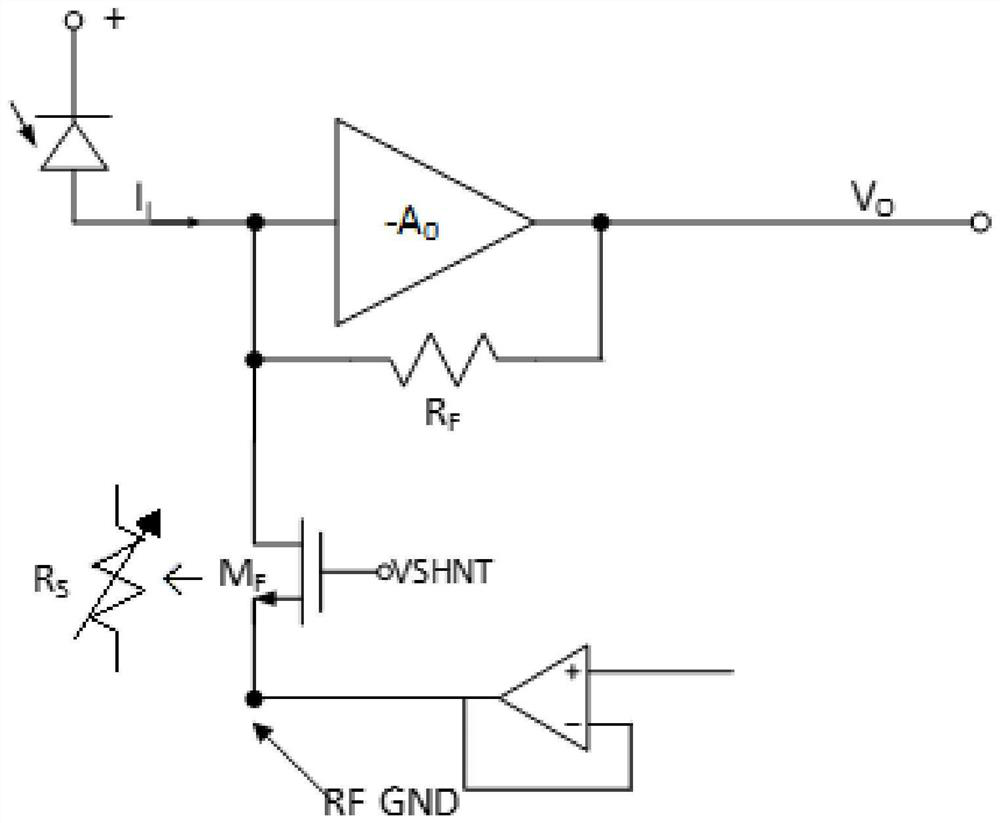
[0044] The peak differential parameter is compared with the reference voltage by a comparator. If the peak differential parameter is greater than or equal to the reference voltage, the first control voltage is output to the gate of the MOSFET transistor, and the MOSF...


PUM


Abstract

The invention discloses a TIA overload current correction method and circuit used in an optical receiver in the technical field of optical communication. The steps of the method include: obtaining two AC voltage signals output by the pseudo-differential transimpedance amplifier circuit; obtaining the current overload signal value through the output two AC voltage signals; comparing the current overload signal value with a preset reference voltage value, and when When the value of the current overload signal is greater than the preset reference voltage value, the current part of one input terminal of the pseudo-differential transimpedance amplifier circuit is shunted to the other input terminal. The beneficial effect of the present invention is that in high-speed circuits and systems, the pseudo-differential TIA AC current is shunted to the virtual GND point instead of the physical GND point, reducing the components in the circuit and reducing the difficulty of circuit component layout; The stability of the TIA is maintained, and the bandwidth of the TIA remains unchanged; from the perspective of virtual GND, the parallel capacitance of the MOS device is halved, thereby reducing the parasitic capacitance.

Description

technical field [0001] The invention relates to the technical field of optical communication, in particular to a TIA overload current correction method and circuit used in an optical receiver. Background technique [0002] In the existing optical communication technology, the optical transmitter uses DP-QPSK, QAM and other methods to modulate the optical signal. After receiving the optical signal, the optical receiver demodulates the optical signal to obtain communication information. The transimpedance amplifier (TIA ) As a key component of the front end of the optical receiver, it has become the focus of research in recent years. Its function is to convert the current output from the photodetector into a voltage and amplify it. When designing a transimpedance amplifier, it is necessary to have as little input current noise as possible; a bandwidth that can match the data transmission speed and a sufficiently large gain. The patent "A Transimpedance Amplifier" (publication...

Claims


Application Information

Patent Timeline
Patent Type & Authority Patents(China)
IPC IPC(8): H03F1/02H03F1/30H03F1/34H03F3/45H03G3/30
CPCH03F1/0211H03F1/301H03F1/342H03F3/45179H03G3/3084
Inventor 维卡斯·马南
Owner 成都英思嘉半导体技术有限公司
Why Eureka
Try Eureka