Micro-nano optical structure
An optical structure, micro-nano technology, applied in the field of micro-nano optics, can solve the problem of weak circular dichroism signal, and achieve the effects of enhanced chirality, strong practicability, and easy detection.
- Summary
- Abstract
- Description
- Claims
- Application Information
AI Technical Summary
Problems solved by technology
Method used
Image
Examples
Embodiment 1
[0032] In order to enhance the circular dichroism of natural molecules, the embodiment of the present application provides a micro-nano optical structure, such as figure 1 As shown, it includes a first metal strip 1, a second metal strip 2, a third metal strip 3 and a fourth metal strip 4, one end of the second metal strip 2 is vertically connected to one end of the first metal strip 1, and the third metal strip 3 The second metal strip 2 and the third metal strip 3 are located at the same side direction of the first metal strip 1 and vertically connected to the other end of the first metal strip 1 . One end of the fourth metal strip 4 is vertically connected to the other end of the third metal strip 3 , and the other end of the second metal strip 2 is vertically connected to the non-end position of the other end of the fourth metal strip 4 .
[0033] The embodiment of the present application provides a micro-nano optical structure with chirality, which can generate large circ...
Embodiment 2
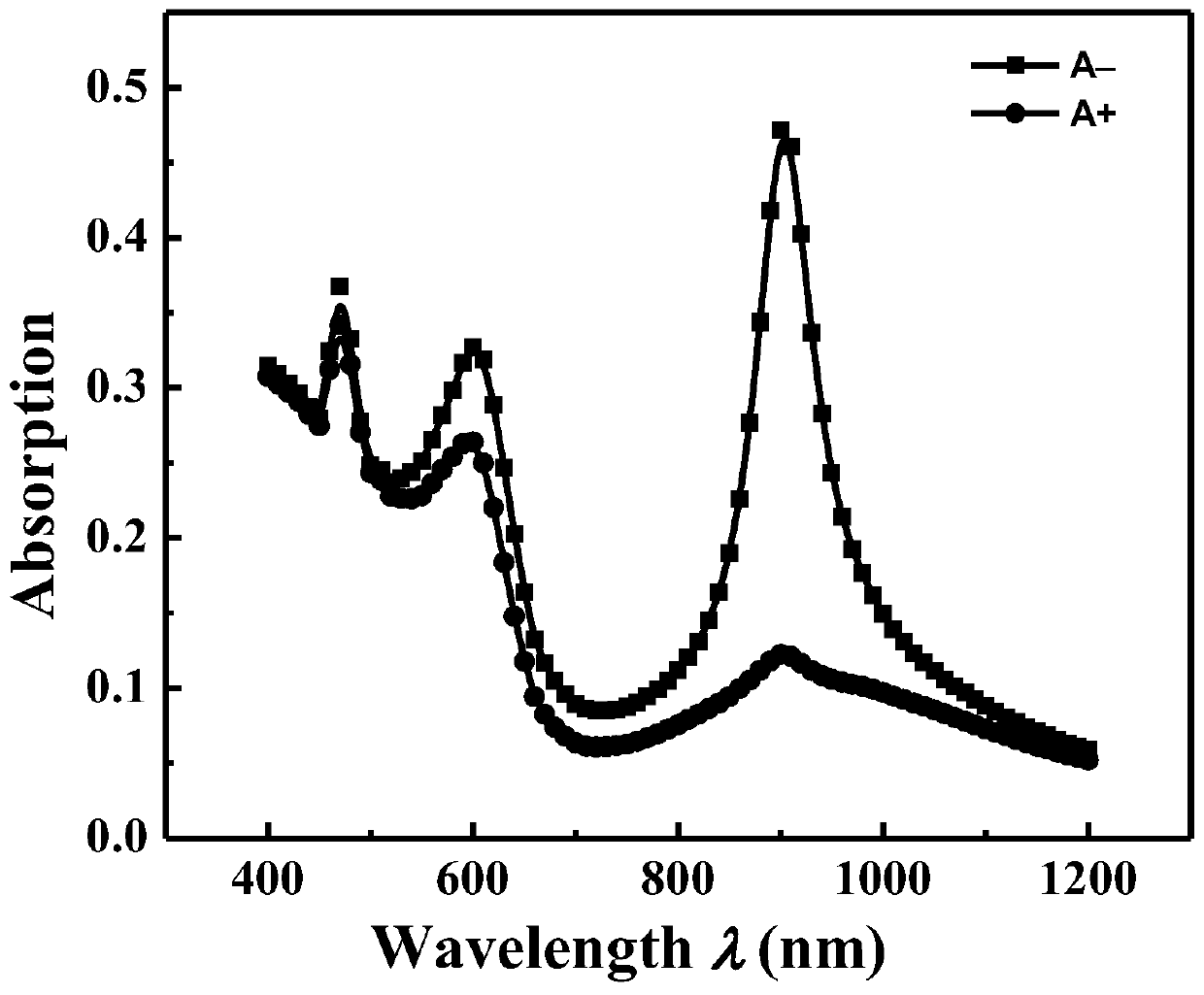
[0037] In order to further illustrate the circular dichroism characteristic of a kind of micro-nano optical structure of embodiment 1, such as Figure 3-Figure 6 As shown, this embodiment discloses its absorption spectrum and circular dichroism spectrum.
[0038] Such as figure 1 As shown, the present embodiment sets the thickness of the micro-nano optical structure h=40nm; the length of the first metal strip 1 is l 1 = second metal strip 2 length l 2 = length l of the third metal strip 3 3 = length l of the fourth metal strip 4 4 =100nm; the first metal strip 1 width W 1 = second metal strip 2 width W 2 =The third metal strip 3 width W 3 = Fourth metal strip 4 width W 4 =20nm; the distance d between the second metal strip 2 and the third metal strip 3=10nm.
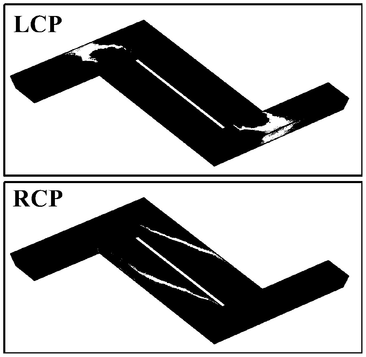
[0039] Such as figure 2 For the charge distribution diagram of this embodiment, from figure 2 We can see that when the left-handed polarized light (LCP) is irradiated, the positive charges are mainly concentr...
PUM
| Property | Measurement | Unit |
|---|---|---|
| thickness | aaaaa | aaaaa |
Abstract
Description
Claims
Application Information
 - Generate Ideas
- Intellectual Property
- Life Sciences
- Materials
- Tech Scout
- Unparalleled Data Quality
- Higher Quality Content
- 60% Fewer Hallucinations
Browse by: Latest US Patents, China's latest patents, Technical Efficacy Thesaurus, Application Domain, Technology Topic, Popular Technical Reports.
© 2025 PatSnap. All rights reserved.Legal|Privacy policy|Modern Slavery Act Transparency Statement|Sitemap|About US| Contact US: help@patsnap.com


