


Quick Research
Generate reliable direction feasibility study reports for your R&D in just a few steps.

Technical Q&A
Discover and master advanced knowledge NOW. Basics, ideas, possibilities, all at once.

Find Solutions
As an expert in R&D theories, this can generate solutions to your technical problems instantly.

Evaluate Feasibility
Analyze your overall solution with one click, know your potential R&D risks in advance.

Monitor Landscape
Get weekly tech updates, stay abreast of the latest tech innovations and key insights.
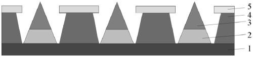
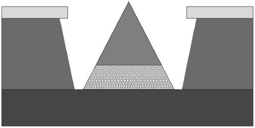
A field emission cathode structure with a flow-limiting resistance variable layer and its preparation method
A field emission cathode and resistive layer technology, which is applied in cold cathode manufacturing, electrode system manufacturing, discharge tube/lamp manufacturing, etc., can solve problems such as device damage and cathode-grid short circuit, and achieve low manufacturing cost and performance improvement , Improve the effect of launch stability
- Summary
- Abstract
- Description
- Claims
- Application Information
AI Technical Summary
Problems solved by technology
Method used
Image


Examples
Embodiment 1
[0032] This embodiment provides a method for preparing a field emission cathode with a flow-limiting resistive layer, comprising the following steps:
[0033] Step A: Wafer Selection and Cleaning
[0034] In this embodiment, P-type lightly doped silicon wafers are selected, and the resistivity is about 3-25Ω / cm -3 , the crystal orientation is 100, using deionized water, ethanol, acetone, SC-1, SC-2, deionized water for ultrasonic cleaning in sequence;
[0035] Step B: Fabrication of Spindt Field Emission Cavity Structure
[0036] The insulating layer is made by the oxidation process, and then the metal gate is made by the sputtering coating process, and then the array pattern is made by the photolithography process and the cavity structure is made by the etching process;
[0037] Step C: Preparing the resistive layer of the metal ion-doped memristive material
[0038] First, a silicon oxide layer (SiO x), and then use sputtering coating process to coat silver film on the s...
Embodiment 2
[0045] This embodiment provides a method for preparing a field emission cathode with a flow-limiting resistive layer, comprising the following steps:
[0046] Step A: Wafer Selection and Cleaning
[0047] In this embodiment, P-type lightly doped silicon wafers are selected, and the resistivity is about 3-25Ω / cm -3 , the crystal orientation is 100, using deionized water, ethanol, acetone, SC-1, SC-2, deionized water for ultrasonic cleaning in sequence;
[0048] Step B: Fabrication of Spindt Field Emission Cavity Structure
[0049] The insulating layer is made by the oxidation process, and then the metal gate is made by the sputtering coating process, and then the array pattern is made by the photolithography process and the cavity structure is made by the etching process;
[0050] Step C: Preparing the resistive layer of the metal ion-doped memristive material
[0051] First, a titanium oxide layer (TiO x ), and then use sputtering coating process to plate silver film on th...
Embodiment 3
[0057] This embodiment provides a method for preparing a field emission cathode with a flow-limiting resistive layer, comprising the following steps:
[0058] Step A: Wafer Selection and Cleaning
[0059] In this embodiment, P-type lightly doped silicon wafers are selected, and the resistivity is about 3-25Ω / cm -3 , the crystal orientation is 100, using deionized water, ethanol, acetone, SC-1, SC-2, deionized water for ultrasonic cleaning in sequence;
[0060] Step B: Fabrication of Spindt Field Emission Cavity Structure
[0061] The insulating layer is made by the oxidation process, and then the metal gate is made by the sputtering coating process, and then the array pattern is made by the photolithography process and the cavity structure is made by the etching process;
[0062] Step C: Preparing the resistive layer of the metal ion-doped memristive material
[0063] First, a LaMnO3 layer (LMO) is deposited in the cavity, and then a copper film is deposited on the LaMnO3 l...
PUM
| Property | Measurement | Unit |
|---|---|---|
| electrical resistivity | aaaaa | aaaaa |
| electrical resistivity | aaaaa | aaaaa |
Abstract
Description
Claims
Application Information
 - R&D Engineer
- R&D Manager
- IP Professional
- Industry Leading Data Capabilities
- Powerful AI technology
- Patent DNA Extraction
Browse by: Latest US Patents, China's latest patents, Technical Efficacy Thesaurus, Application Domain, Technology Topic, Popular Technical Reports.
© 2024 PatSnap. All rights reserved.Legal|Privacy policy|Modern Slavery Act Transparency Statement|Sitemap|About US| Contact US: help@patsnap.com