A Tunable Waveguide Grating Surface Emitter

A technology of waveguide grating and grating surface, which is applied to optical waveguides, instruments, optics, etc., can solve the problems of reducing the heating efficiency of thermo-optic devices, low thermal conductivity of isolation layers, and limiting the speed of thermo-optic regulation, and achieves convenient design and thermal conductivity. The effect of high coefficient and lower production cost

Active Publication Date: 2020-05-19
ZHEJIANG UNIV
View PDF6 Cites 0 Cited by
  • Summary
  • Abstract
  • Description
  • Claims
  • Application Information

AI Technical Summary

Problems solved by technology

Since the thermal conductivity of the isolation layer is generally relatively low, it is not conducive to conduct heat to the optical waveguide after the electrodes are energized, thereby reducing the heating efficiency of the thermo-optic device and limiting the speed of thermo-optic regulation.

Method used


Image

  • A Tunable Waveguide Grating Surface Emitter
  • A Tunable Waveguide Grating Surface Emitter
  • A Tunable Waveguide Grating Surface Emitter

Examples


Embodiment 1

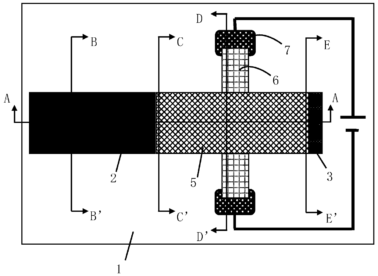
[0050] Only a single core strip optical waveguide and a micro-graphene heater are arranged, such as figure 1 shown.

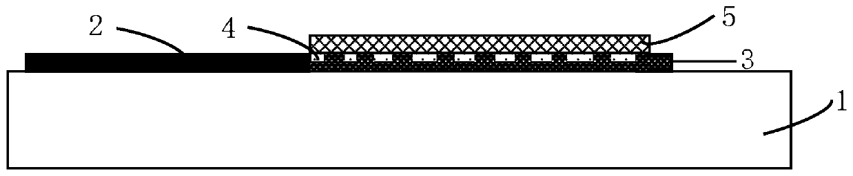
[0051] The silicon nanowire optical waveguide based on silicon insulator (SOI) material is selected: the core layer is silicon material, the thickness is 220nm, and the refractive index is 3.4744; the lower cladding material is silicon dioxide, the thickness is 2μm, and the refractive index is 1.4404; The upper cladding material is air, and the refractive index is approximately 1. Considering that the incident center wavelength is 1550nm, the TE polarization mode is adopted.

[0052] The core layer is etched into a strip waveguide with a certain width by photolithography and other processes, and the coupling grating is etched at the front end to couple the light in the fiber into the silicon waveguide. The end is also etched into a grating structure, but the size of the coupling grating is different. different. The etching depth is 0.065 μm, the period is 0....

Embodiment 2

[0057] Such as Figure 8 and Figure 9 As shown, the specific implementation includes multiple core layer strip optical waveguides and only one micro-graphene heater, multiple core layer strip optical waveguides are arranged in parallel on the lower cladding layer, and the micro-graphene heaters are laid on the common multiple cores On the grating diffraction area of ​​the strip optical waveguide, multiple grating diffraction areas are cascaded. Here, in order to make the graphene pavement smoother, after the input waveguide and waveguide grating are etched, HSQ photoresist is used to fill the grating etching area and the interval area between adjacent waveguides. Due to the increase of the graphene area, higher power is required to increase the waveguide to the same temperature, and the heating efficiency is lower than that of Example 1. The same mode light is input into each waveguide, but the adjacent waveguides maintain a fixed phase difference (the phase difference can ...


PUM

PropertyMeasurementUnit
thicknessaaaaaaaaaa
thicknessaaaaaaaaaa
depthaaaaaaaaaa

Abstract

The invention discloses a tunable waveguide grating surface transmitter. A waveguide grating structure is connected to the output end of an input optical waveguide and provided with a grating groove filled with a filling material; a square graphene layer is laid on the top surface of the waveguide grating structure, metal electrodes are arranged on the sides of a grating diffraction area, the metal electrodes on the two sides are connected to the square graphene layer through strip graphene connecting arms, the metal electrodes are connected to the two ends of an external power circuit, and the external power circuit applies voltage to form a passage through the metal electrodes, the strip graphene connecting arms and the square graphene layer; and the square graphene layer is used as a main heating area to heat the waveguide grating structure to regulate and control a grating diffraction angle, and the mode light transmitted in the waveguide is diffracted out towards the upper part ofthe waveguide through the grating diffraction area. According to the invention, the grating diffraction angle is regulated and controlled by regulating the voltages at the two ends of the graphene, the structure is simple, and the optical waveguide phased array laser radar which is small in size, low in cost and high in regulation and control speed is expected to be realized.

Description

technical field [0001] The invention relates to a tunable waveguide grating surface emitter, in particular to a hybrid integrated tunable waveguide grating surface emitter using graphene as a heater. Background technique [0002] The laser radar uses a moving laser beam to scan and sample the detection target to obtain the position, speed and other characteristic quantities of the detection target. The traditional mechanical lidar scans the space by mechanical rotation. This method has a slow response speed, and the machinery is easy to age and has poor reusability. At the same time, the entire device is bulky and inconvenient to transport and carry. In contrast, phased-array lidar, which has been widely studied in recent years, can change the emission direction of laser beams by adjusting the relative phase of multiple signals, and has the advantages of fast response speed and small size. [0003] With the increasing development of photonic integration technology, optical ...

Claims


Application Information

Patent Timeline
Patent Type & Authority Patents(China)
IPC IPC(8): G02B6/12G02B6/124H05B3/14H05B3/03
CPCG02B6/12004G02B6/124G02B2006/12085G02B2006/12107H05B3/03H05B3/141
Inventor 戴道锌孙仪
Owner ZHEJIANG UNIV
Why Eureka
Try Eureka