Perovskite solar cell taking organic amine as an interface modification layer and preparation method thereof
A technology for interface modification layers and solar cells, which can be applied in circuits, photovoltaic power generation, electrical components, etc., and can solve problems that affect the stability and photoelectric conversion efficiency of perovskite cells, van der Waals force or weak hydrogen bond, weak force, etc. , to achieve the effects of improving photoelectric conversion efficiency, improving charge collection efficiency, and improving affinity
- Summary
- Abstract
- Description
- Claims
- Application Information
AI Technical Summary
Problems solved by technology
Method used
Image
Examples
preparation example Construction
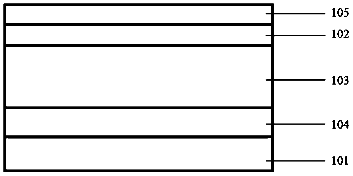
[0027] The present invention also provides a method for preparing the above-mentioned perovskite solar cell using an organic amine as an interface modification layer, comprising:
[0028] 1) Prepare an electron transport layer or a hole transport layer on the transparent conductive layer;
[0029] 2) depositing the hydroxyl-containing organic amine solution on the electron transport layer or the hole transport layer to obtain an interface modification layer;
[0030] 3) Prepare a perovskite absorber layer on the interface modification layer;
[0031] 4) preparing a hole transport layer or an electron transport layer on the perovskite absorber layer;
[0032] 5) A back electrode layer is prepared on the hole transport layer or the electron transport layer.
[0033] The preparation method of the interface modification layer adopts the method of spin coating a hydroxyl-containing organic amine solution, wherein the concentration of the hydroxyl-containing organic amine solution...
Embodiment 1
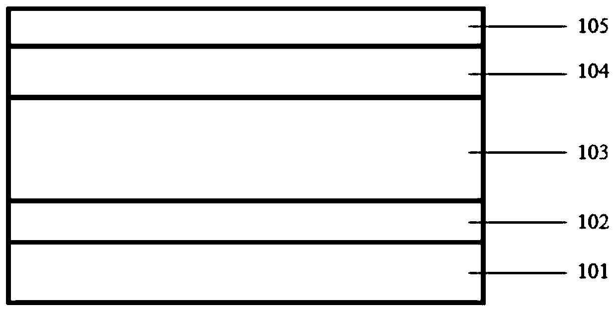
[0047] like figure 1 The formal structure diagram of the perovskite solar cell shown, and the specific preparation method is as follows:
[0048] 1) Clean the FTO conductive substrate with a thickness of 80 nm.
[0049] 2) Spin-coating SnO on FTO conductive substrate 2 Aqueous solution, annealed at 180 °C to obtain an electron transport layer with a thickness of 100 nm.
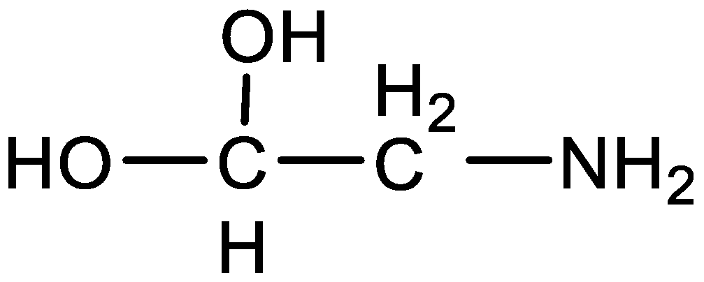
[0050] 3) Spin-coat (OH) at a concentration of 2 mM on the electron transport layer 2 CHCH 2 NH 2 (Structure like image 3 shown) aqueous solution, the spin coating speed was 3000 rpm, the spin coating time was 20 s, and annealed at 100 °C to obtain an interface modification layer with a thickness of 10 nm.
[0051] 4) Preparation of PbI 2 The DMF / DMSO mixture (V DMF :V DMSO =9:1) and the isopropanol mixed solution of FAI, MABr, MAC1;
[0052] Spin-coating PbI on the interface modification layer 2 The DMF / DMSO mixture was annealed at 70 °C to obtain PbI 2 film layer;
[0053] in PbI 2 The mixed ...
Embodiment 2
[0057] like figure 1 The formal structure diagram of the perovskite solar cell shown, and the specific preparation method is as follows:
[0058] The specific preparation steps are as described in Example 1, except that:
[0059] 3) Spin coating (OH) at a concentration of 0.05 mM on the electron transport layer 2 CHCH 2 NH 2 (Structure like image 3 shown) aqueous solution, spin coating speed of 4000 rpm, spin coating time of 10 s, and annealing at 100 °C to obtain an interface modification layer with a thickness of 5 nm.
PUM
 Abstract
Description
Claims
Application Information
 - R&D Engineer
- R&D Manager
- IP Professional
- Industry Leading Data Capabilities
- Powerful AI technology
- Patent DNA Extraction
Browse by: Latest US Patents, China's latest patents, Technical Efficacy Thesaurus, Application Domain, Technology Topic, Popular Technical Reports.
© 2024 PatSnap. All rights reserved.Legal|Privacy policy|Modern Slavery Act Transparency Statement|Sitemap|About US| Contact US: help@patsnap.com


