Preparation method of single crystal thin film bulk acoustic wave resonator and bulk acoustic wave resonator
A bulk acoustic wave resonator, single crystal thin film technology, applied in the manufacture/assembly of piezoelectric/electrostrictive devices, piezoelectric/electrostrictive/magnetostrictive devices, electrical components, etc., can solve the problem of single crystal thin film layer Cracks, single crystal thin-layer film lifting, depressions and other problems, to simplify the preparation steps, ensure device performance, and simplify the opening process.
- Summary
- Abstract
- Description
- Claims
- Application Information
AI Technical Summary
Problems solved by technology
Method used
Image
Examples
preparation example Construction
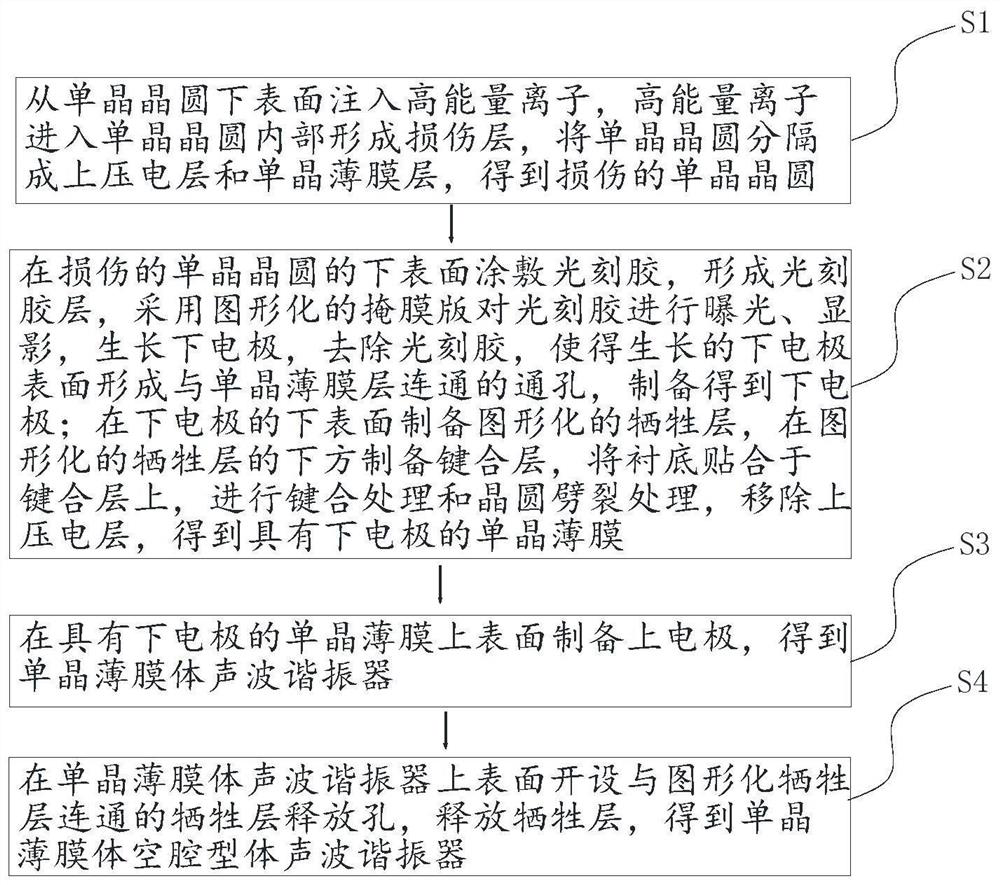
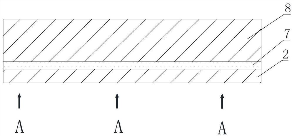
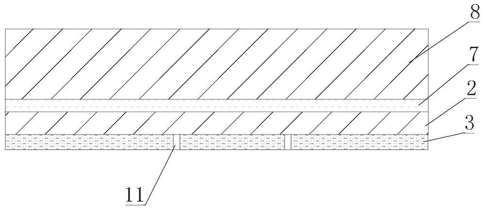
[0054] Such as figure 1 , figure 2 , image 3 , image 3 , Figure 5 and Figure 6 As shown, the present invention provides a kind of preparation method of monocrystalline thin film bulk acoustic resonator, comprises the steps:
[0055] S1) High-energy ions A are injected from the lower surface of the single-crystal wafer, and the high-energy ions A enter the interior of the single-crystal wafer to form a damaged layer 7, and the single-crystal wafer is separated into an upper piezoelectric layer 8 and a single-crystal thin film layer 2, and the obtained Damaged single crystal wafers;
[0056] S2) Coating photoresist on the lower surface of the damaged single crystal wafer to form a photoresist layer, using a patterned mask to expose and develop the photoresist, growing the lower electrode, preparing the lower electrode, removing photoresist, so that the surface of the grown lower electrode forms a patterned through hole 11 connected to the single crystal thin film laye...
Embodiment 1
[0100] The preparation of a lithium niobate single crystal thin-film cavity-type bulk acoustic wave resonator by method 1 includes the following steps:
[0101] 1) A lithium niobate single crystal wafer is selected, and high-energy helium ions (He 2 +), so that a damage layer is formed inside the lithium niobate single crystal wafer, and the damage layer separates the lithium niobate single crystal wafer into a lithium niobate upper piezoelectric layer and a lithium niobate single crystal film layer; He 2 + The implantation energy is 200keV, and the implantation depth is 0.6μm;
[0102] 2) Coating photoresist (Ruihong AZ6212) on the lower surface of the lithium niobate single crystal thin film layer to form a photoresist layer, and using a patterned mask (made of chromium) to expose and develop the photoresist , grow the Pt lower electrode, and use acetone to clean and remove the photoresist, so that the surface of the grown Pt lower electrode forms a through hole connected w...
Embodiment 2
[0108] The preparation of a lithium tantalate single crystal thin-film cavity-type bulk acoustic wave resonator by method 1 includes the following steps:
[0109] 1) A lithium tantalate single crystal wafer is selected, and high-energy helium ions (He 2 +), so that a damage layer is formed inside the lithium tantalate single crystal wafer, and the damage layer separates the lithium tantalate single crystal wafer into a piezoelectric layer on lithium tantalate and a lithium tantalate single crystal film layer; He 2 + The implantation energy is 500keV, and the implantation depth is 0.6μm;
[0110] 2) Coating photoresist (Ruihong AZ6212) on the lower surface of the lithium tantalate single crystal film layer to form a photoresist layer, and using a patterned mask (made of chromium) to expose and develop the photoresist , grow the Pt lower electrode, and use acetone to clean and remove the photoresist, so that the surface of the grown Pt lower electrode forms a through hole conne...
PUM
| Property | Measurement | Unit |
|---|---|---|
| thickness | aaaaa | aaaaa |
| thickness | aaaaa | aaaaa |
| thickness | aaaaa | aaaaa |
Abstract
Description
Claims
Application Information
 - R&D
- Intellectual Property
- Life Sciences
- Materials
- Tech Scout
- Unparalleled Data Quality
- Higher Quality Content
- 60% Fewer Hallucinations
Browse by: Latest US Patents, China's latest patents, Technical Efficacy Thesaurus, Application Domain, Technology Topic, Popular Technical Reports.
© 2025 PatSnap. All rights reserved.Legal|Privacy policy|Modern Slavery Act Transparency Statement|Sitemap|About US| Contact US: help@patsnap.com


