Method for improving growth efficiency of silicon carbide crystals

A technology of crystal growth and silicon carbide, applied in crystal growth, single crystal growth, single crystal growth, etc., can solve the problems of complex cleaning of the upper cover, waste of silicon carbide sources, failure of silicon carbide sources to grow, etc.

Inactive Publication Date: 2019-07-12
ZHEJIANG EAST CRYSTAL BOLANTE PHOTOELECTRIC
View PDF0 Cites 4 Cited by
  • Summary
  • Abstract
  • Description
  • Claims
  • Application Information

AI Technical Summary

Problems solved by technology

In general crucible design, the seed crystal and crucible top cover are designed flat, and the side wall of the crucible is a vertical structure. Therefore, when the crucible is heated by induction, the top cover around the seed crystal and the top of the crucible are relatively low temperature relative to the SiC source, resulting in long During crystallization, the seed crystal and its surroundings are prone to sublimation atomic crystallization, which will cause non-dose-ratio silicon carbide sources to be unable to effectively grow on the seed crystal, resulting in waste of silicon carbide sources and complicated cleaning of the crucible and upper cover after crystal growth.

Method used


Image

  • Method for improving growth efficiency of silicon carbide crystals
  • Method for improving growth efficiency of silicon carbide crystals

Examples


Embodiment Construction

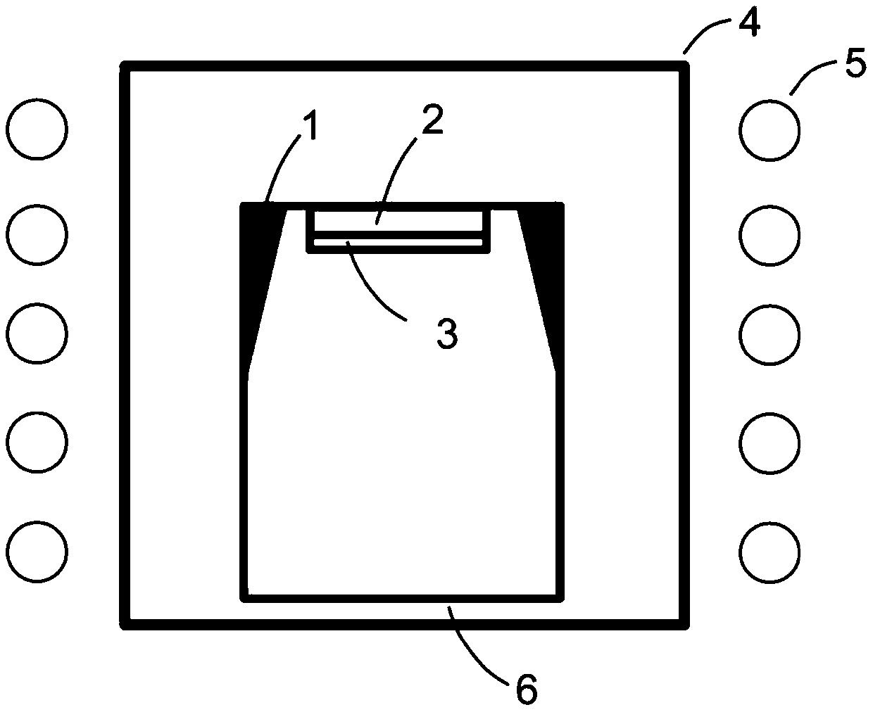
[0008] The inclined chamfer inside the crucible is processed by computer numerical control technology (CNC) to produce a concave inclined surface, and the inclined surface is presented along the inner side of the upper mouth of the crucible in a complete circle. The inclined surface extends toward the bottom of the crucible, so as to achieve a form in which the upper wall of the crucible is thick and the lower wall is thin.

[0009] The angled crucible with concave inclined surface can be concave, flat or convex. The extension length to the bottom of the crucible can be 1 / 8 to 7 / 8 of the height of the crucible. The plane angle is between 10° and 35°. The range of concave and convex surfaces shall not exceed 1 / 8 of the crucible diameter.

[0010] The inclined angle in the crucible can effectively reduce the temperature gradient difference between the seed crystal and the angle, which is 50% to 80% smaller than the traditional physical vapor transport method, reducing the atta...


PUM

PropertyMeasurementUnit
melting pointaaaaaaaaaa

Abstract

The invention discloses a method for improving growth efficiency of silicon carbide crystals. A device for realizing the method comprises a lead angle crucible for growing silicon carbide single crystals, an induction heating coil, a heat preservation system and a seed crystal. According to the method provided by the invention, when the silicon carbide crystals are grown, lead angles of the edge of the crucible have the following effects: 1, the lead angles improve the temperature gradient close to the seed crystal; 2, the lead angles guide volatile atoms to the low-temperature seed crystal; 3, the lead angles reduce crystallization of the volatile atoms at the lead angle position; and 4 the lead angles improve length of the grown crystals.

Description

technical field [0001] The invention belongs to the field of semiconductors and relates to silicon carbide crystal growth, crucible design and thermal field of a crystal growth furnace. Background technique [0002] Silicon carbide, the third-generation semiconductor, is a single crystal grown at high temperature, its hardness is second only to diamond, and its melting point is 2830°C. Difficult growth conditions, resulting in expensive silicon carbide crystal cost. Silicon carbide substrates made of silicon carbide crystals are widely used in electronic power devices and nitride epitaxial growth, and can be widely used in electric vehicles, hybrid vehicles, rail transit, high-frequency devices, microwave devices, etc., with very high economic benefits and national defense value. [0003] From the silicon-carbon binary phase diagram, it is known that silicon carbide growth crystals cannot be directly solidified from a single liquid because of their high melting point, and c...

Claims


Application Information

Patent Timeline
Patent Type & Authority Applications(China)
IPC IPC(8): C30B23/00C30B29/36
CPCC30B23/00C30B29/36
Inventor 徐良蓝文安占俊杰阳明益刘建哲余雅俊
Owner ZHEJIANG EAST CRYSTAL BOLANTE PHOTOELECTRIC
Why Eureka
Try Eureka