All-inorganic perovskite micron sheet and preparation method thereof, and Schottky ultraviolet photoelectric detector and preparation method thereof
A technology of electrical detectors and micro-sheets, which is applied in the preparation of micro-sheets and detectors, and in the field of Schottky ultraviolet photodetectors. The effect of simple operation process
- Summary
- Abstract
- Description
- Claims
- Application Information
AI Technical Summary
Problems solved by technology
Method used
Image
Examples
Embodiment 1
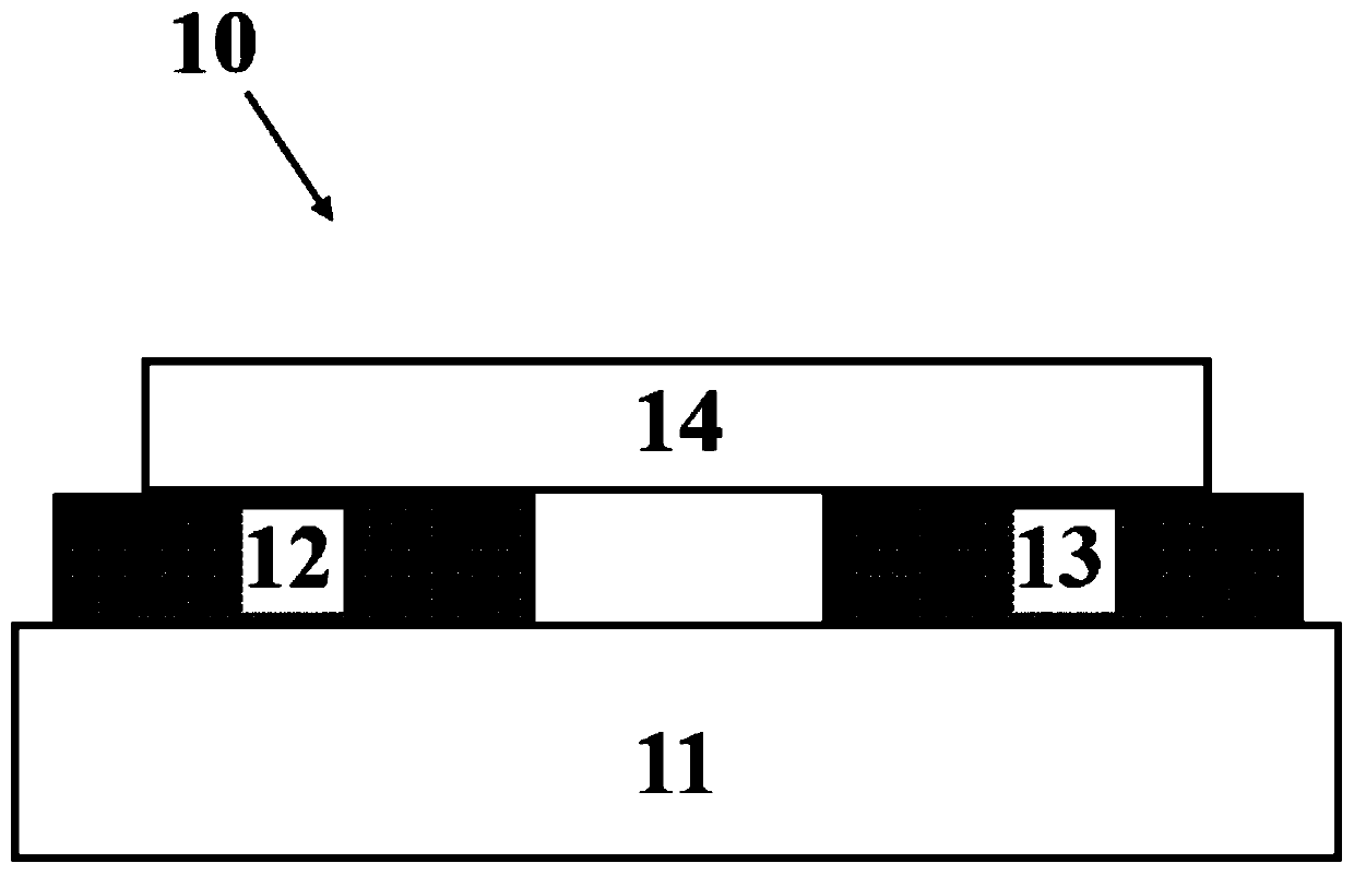
[0041] Such as figure 1 As shown, the preparation method of the Schottky type ultraviolet photodetector 10 provided in this embodiment comprises the following steps:
[0042] 1. Substrate cleaning
[0043] The substrate can be Si / SiO 2 , glass, ITO and GaN and other substrates, Si / SiO is used in this embodiment 2 Substrate, first cut the substrate into a suitable size (1cm×1cm), then use deionized water, acetone, absolute ethanol, and deionized water to ultrasonically clean it in an ultrasonic cleaner for 10 minutes, and then blow it with nitrogen. Dry to get a clean substrate.
[0044] 2. Preparation of ITO electrodes with left and right structures
[0045] ITO electrodes are mainly prepared by photolithography and magnetron sputtering techniques.
[0046] (1) Photolithography: First, use a homogenizer to evenly spin-coat the photoresist on the clean Si / SiO 2 On the substrate, the condition is to rotate at a low speed of 600 rpm for 6 seconds, and then rotate at a high ...
Embodiment 2
[0057] The difference between the preparation method of the Schottky-type ultraviolet photodetector provided in the second embodiment and the first embodiment is only in "preparation of all-inorganic perovskite microsheets", specifically:
[0058] Prepare CsPbCl with a concentration of 0.01mol / L 3 / DMSO solution, and then grown on a hot stage at 70 °C for 96 hours, as Figure 7 As shown, it can be observed that there is CsPbCl on the substrate 3 Formation of microflakes with a size of 10 x 10 microns and a thickness of 300 nm.
[0059] The rest of the process is the same as that of Embodiment 1, and will not be repeated here.
[0060] test:
[0061] The prepared CsPbCl 3 The perovskite microsheet sample is placed on the probe station, and the scanning voltage is applied to the left and right electrodes to obtain dark current and photocurrent under 400nm monochromatic light, such as Figure 8 shown.
Embodiment 3
[0063] The difference between the preparation method of the Schottky-type ultraviolet photodetector provided in the third embodiment and the first embodiment is only in "preparation of all-inorganic perovskite microsheets", specifically:
[0064] Prepare CsPbCl with a concentration of 0.1mol / L 3 / DMSO solution, and then grown on a hot stage at 30 °C for 12 hours, as Figure 9 As shown, it can be observed that there is CsPbCl on the substrate 3 Formation of microflakes with a size of 20 x 30 microns and a thickness of 800 nm.
[0065] The rest of the process is the same as that of Embodiment 1, and will not be repeated here.
[0066] test:
[0067] The prepared CsPbCl 3 The perovskite microsheet sample is placed on the probe station, and the scanning voltage is applied to the left and right electrodes to obtain dark current and photocurrent under 400nm monochromatic light, such as Figure 10 shown.
[0068] The data obtained in the above examples show that the all-inorgan...
PUM
| Property | Measurement | Unit |
|---|---|---|
| Size | aaaaa | aaaaa |
| Thickness | aaaaa | aaaaa |
Abstract
Description
Claims
Application Information
 - R&D
- Intellectual Property
- Life Sciences
- Materials
- Tech Scout
- Unparalleled Data Quality
- Higher Quality Content
- 60% Fewer Hallucinations
Browse by: Latest US Patents, China's latest patents, Technical Efficacy Thesaurus, Application Domain, Technology Topic, Popular Technical Reports.
© 2025 PatSnap. All rights reserved.Legal|Privacy policy|Modern Slavery Act Transparency Statement|Sitemap|About US| Contact US: help@patsnap.com


