A Formally Mounted Integrated Unit Diode Chip
一种集成单元、二极管的技术,应用在电气元件、半导体器件、电路等方向,能够解决LED光效、散热和稳定性限制等问题,达到提升光萃取效率、大散热面积、佳散热性能的效果
- Summary
- Abstract
- Description
- Claims
- Application Information
AI Technical Summary
Problems solved by technology
Method used
Image
Examples
Embodiment 1
[0049] This embodiment provides a 6V high-voltage integrated unit light-emitting diode chip design, such as Figure 12-13 As shown, every two chip units are connected in series with each other to form a 6V high-voltage chip unit, and each 6V high-voltage chip unit is connected in parallel with each other. At this time, the ratio of series-parallel connection is 1:1. The units are connected in series with each other, and then connected in parallel with other N chip units. At this time, the ratio of series-parallel connection is 1:N. The circuit diagram is as follows Figure 12 shown.
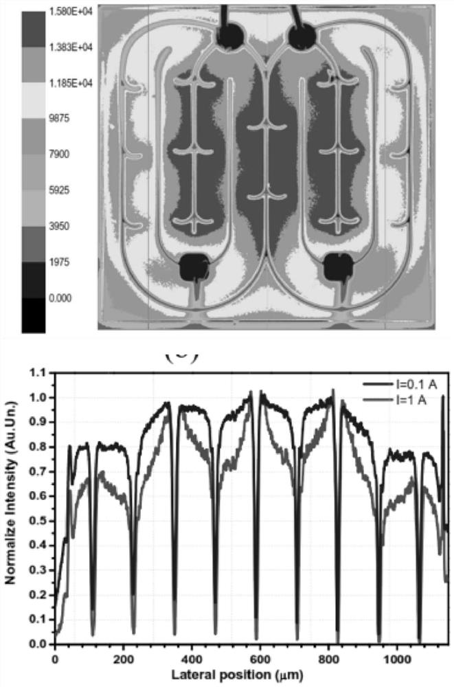
[0050] Such as Figure 13 As shown, the 6V high-voltage chip units are insulated from each other, and the n-type gallium nitride (n-GaN) platform 7 is exposed for each unit, and the left chip is connected in series through the bridge metal in the middle. The n-electrode and the p-electrode of the chip on the right. The 6V chip units are connected in parallel with each other, so even if a certa...
Embodiment 2
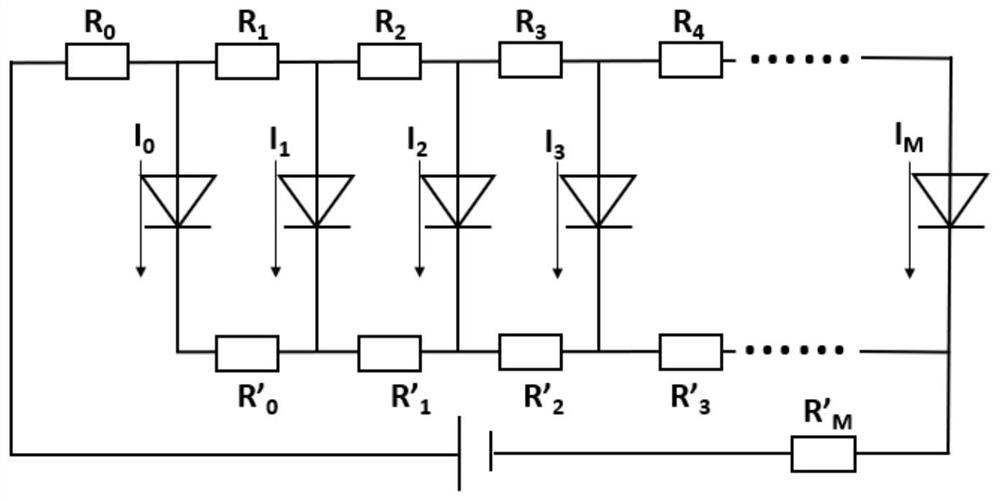
[0054] This embodiment provides a formal integration design method, image 3 It is a schematic circuit diagram of the unit diode chip series structure of the present invention.
[0055] where R 0 , R 1 , R 2 , R 3 , R 4 ... is the resistance from the P-type electrode electrode line between a plurality of unit diode chips to the quantum well active region; R' 0 ,R′ 1 ,R′ 2 ,R′ 3 ,R′ 4 …for multiple unit diode chips between
[0056]
[0057] The resistance of the N-type electrode electrode line to the active region of the quantum well. Usually in the Nth unit diode chip, R N = R NM +R Nc +R Np-GaN , where R NM is the electrode wire resistance of the P-type electrode, R Nc is the contact resistance of a p-type ohmic contact, R Np-GaN is the resistance of p-GaN material; similarly, in the Nth unit diode chip, R′ N =R' NM +R' Nc +R' Nn-GaN , where R'NM is the N-type electrode wire resistance, R' Nc is the contact resistance of n-type ohmic contact, R' Nn-G...
Embodiment 3
[0066] This embodiment provides a positively mounted integrated unit diode chip, the mesa structure area of which is determined according to the current, such as Figure 5 to Figure 7 As shown, it includes N-type electrode 1 , P-type electrode 2 , ITO 3 , hole 11 , N-type electrode line 12 , and P-type electrode line 13 .
[0067] In the unit diode chip, the length of the diode unit row is fixed as L, and the diode units from the P-type electrode to the right are defined in sequence, and their widths are defined as L 0 , L 1 , L 2 , L 3 ,... L N …L M ; where the width of the diode unit satisfies L 0 >L 1 >L 2 >L 3 >…>L N ...> L M , the optimal design approximation is:
[0068]
[0069] According to L N And the area calculation formula to calculate the area of the table structure.
[0070] In this embodiment, the front sectional view of the hole structure is added as Figure 5 As shown, the pore structure includes a plurality of pore units, the number of pore...
PUM
| Property | Measurement | Unit |
|---|---|---|
| diameter | aaaaa | aaaaa |
| length | aaaaa | aaaaa |
| width | aaaaa | aaaaa |
Abstract
Description
Claims
Application Information
 - Generate Ideas
- Intellectual Property
- Life Sciences
- Materials
- Tech Scout
- Unparalleled Data Quality
- Higher Quality Content
- 60% Fewer Hallucinations
Browse by: Latest US Patents, China's latest patents, Technical Efficacy Thesaurus, Application Domain, Technology Topic, Popular Technical Reports.
© 2025 PatSnap. All rights reserved.Legal|Privacy policy|Modern Slavery Act Transparency Statement|Sitemap|About US| Contact US: help@patsnap.com


