
A one-time programmable non-volatile fuse memory cell

A memory cell, non-volatile technology, applied in the field of one-time programmable non-volatile fuse memory cells

Active Publication Date: 2019-06-18
CHANGXIN MEMORY TECH INC
View PDF5 Cites 0 Cited by
  • Summary
  • Abstract
  • Description
  • Claims
  • Application Information

AI Technical Summary

Problems solved by technology

[0004] Embodiments of the present invention provide a one-time programmable non-volatile fuse storage unit to solve or alleviate one or more technical problems in the prior art

Method used


Image

  • A one-time programmable non-volatile fuse memory cell
  • A one-time programmable non-volatile fuse memory cell
  • A one-time programmable non-volatile fuse memory cell

Examples


Embodiment 1

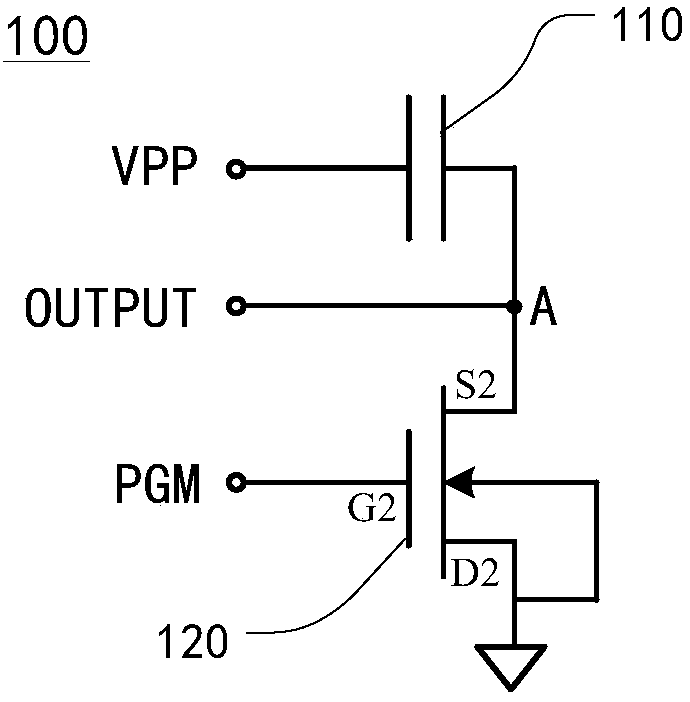
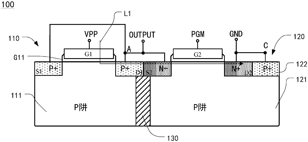
[0051] Such as figure 1 As shown, the OTP non-volatile fuse storage unit 100 of the embodiment of the present invention includes an accumulation type MOS transistor varactor 110 and a selection transistor 120 .

[0052] In this embodiment, the accumulator MOS transistor varactor 110 is a PMOS transistor (PMOSin pwell) formed in a P well (pwell), its gate G1 is connected to the programming voltage VPP, and its source S1 and drain D1 are connected together , and form the first connection point A, the first connection point A is the output port OUTPUT of the storage unit 100, which is used to detect the current passing through the accumulative MOS transistor varactor 110 to output the logic level value "0" or "1 ”, for example, when no current flows through the accumulator MOS transistor varactor 110, the output logic level value of OUTPUT is “0”.

[0053] When the programming voltage VPP applied to the gate G1 of the accumulative MOS transistor varactor 110 is higher than the t...

Embodiment 2

[0061] Such as Figure 4 As shown, the embodiment of the present invention provides an OTP non-volatile fuse storage unit 200 including an accumulation type MOS transistor varactor 210 and a selection transistor 120 . The memory unit 200 in the embodiment of the present invention can be implemented by a CMOS process.

[0062] The accumulative MOS transistor varactor 210 of the embodiment of the present invention is an NMOS transistor (NMOS in nwell) formed in an N well (NWELL) 211, its gate G3 is connected to the programming voltage VPP, and its source S3 and drain S3 are connected Together, and form the first connection point B, the first connection point B is the output port OUTPUT of the storage unit 200, which is used to detect the current passing through the accumulation type MOS transistor varactor 210 to output a logic level value "0" or "1".

[0063] When the programming voltage VPP applied to the grid G3 of the accumulative MOS transistor varactor 210 is higher than...


PUM


Abstract

The invention provides: an OTP non-volatile fuse memory cell, which comprises a cumulative MOS transistor varactor, of which the grid electrode is connected to a programming voltage, and the source electrode and the drain electrode are connected together to form a first connection point; a selection transistor, wherein The grid electrode of the selection transistor is connected to the control signal, the source electrode of the selection transistor is connected to the first connection point, and the drain electrode of the selection transistor is grounded; When the selection transistor is controlled by the control signal to be turned on, a programming voltage greater than a threshold voltage is applied to the gate of the cumulative MOS transistor varactor and maintained for a predeterminedperiod of time to change at least one physical characteristic of the cumulative MOS transistor varactor, thereby changing a logic level output by the first connection point. According to the OTP nonvolatile fuse memory cell, the OTP can be achieved through the fuse principle, no extra mask is needed, the requirements of different manufacturing processes of the CMOS technology can be met, and diversified OTP solutions are provided.

Description

technical field [0001] The invention relates to the technical field of semiconductors, in particular to a one-time programmable non-volatile fuse storage unit. Background technique [0002] OTP (One Time Programmable) one-time programmable memory can only be programmed once and cannot be erased by electricity. It can be applied to program code memory, serial configuration memory, System-on-Chip (SOC for short), etc. , for ID identification, correction, etc. [0003] In the prior art, the OTP is mostly implemented based on the logic architecture of an antifuse, for example, ONO (oxide-silicide-oxide) or MOM (metal-oxide-metal) is used to implement the antifuse. The anti-fuse has a very high resistance before programming, about several hundred megohms, and is broken down by high voltage during programming, and the resistance is reduced to a thousand ohm level or even lower, so as to realize the OTP function. However, both the ONO and MOM structures require an additional mask...

Claims


Application Information

Patent Timeline
Patent Type & Authority Applications(China)
IPC IPC(8): G11C17/16G11C17/18
Inventor 洪根刚
Owner CHANGXIN MEMORY TECH INC
Learn More