
A three-dimensional flash memory array unit operation method with variable programming stages

A technology of unit operation and flash memory array, which is applied in the field of three-dimensional flash memory array unit operation, can solve problems such as the description of multi-valued storage implementation methods, and achieve the effect of narrow spatial distribution

Active Publication Date: 2019-06-18
HUAZHONG UNIV OF SCI & TECH
View PDF11 Cites 3 Cited by
  • Summary
  • Abstract
  • Description
  • Claims
  • Application Information

AI Technical Summary

Problems solved by technology

[0003] The three-dimensional vertical NAND storage string was first disclosed in 2001, however, each cell of this NAND storage string can only store one bit of data
However, the patent does not describe the implementation method of multi-value storage

Method used


Image

  • A three-dimensional flash memory array unit operation method with variable programming stages
  • A three-dimensional flash memory array unit operation method with variable programming stages
  • A three-dimensional flash memory array unit operation method with variable programming stages

Examples


Embodiment Construction

[0028] In order to make the object, technical solution and advantages of the present invention clearer, the present invention will be further described in detail below in conjunction with the accompanying drawings and embodiments. It should be understood that the specific embodiments described here are only used to explain the present invention, not to limit the present invention.

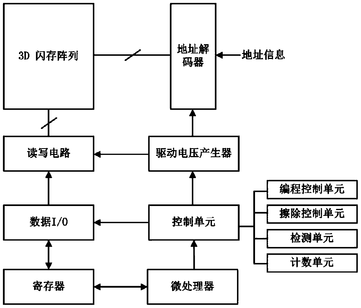
[0029] Such as figure 1 As shown, when performing an erase operation, the microprocessor controls the erase control unit to send an erase command, and controls the address information to be written into the address decoder, controls the drive voltage generator to generate a voltage drive signal (erase voltage), and finally passes the read The write circuit performs an erase operation on the selected block structure. After the erase operation of the selected block structure is completed, the detection control unit and the count control unit sequentially gate and verify the states of different flash...


PUM


Abstract

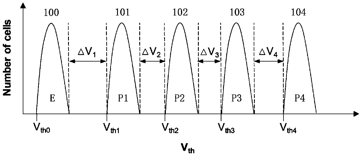
The invention discloses an operation method of a three-dimensional flash memory array unit with variable programming stages. The operation method comprises the following steps: S1, receiving an erasing operation instruction and address information; S2, erasing the selected block structure; S3, receiving a multi-level programming instruction and address information; S4, judging whether the addressoverflows or not, if yes, entering S5, otherwise, receiving programming level information of the target unit, and entering S6; S5, completing the programming operation of the selected block structure,and ending; S6, performing multi-level programming operation on the current flash memory unit according to the multi-level programming instruction, the address information and the programming level information of the target unit; S7, judging whether the difference of the threshold voltages is not smaller than the preset minimum interval voltage or not, if yes, changing the address information, entering S3, and performing the programming operation of the next flash memory unit; And otherwise, carrying out multi-level programming operation on the current flash memory unit for no more than the preset number of times again. The flash memory unit is subjected to target stage number programming, the threshold voltage of the flash memory unit is accurate to the preset value, and therefore the data state of the flash memory unit is accurately controlled.

Description

technical field [0001] The invention belongs to the technical field of semiconductor storage, and more specifically relates to a method for operating a three-dimensional flash memory array unit with variable programming levels. Background technique [0002] Flash memory (Flash), as a non-volatile memory, can be divided into NAND flash memory and NOR flash memory. Each memory cell of NOR flash memory is independently connected to the bit line and word line, so it has good random storage characteristics, and multiple memory cells of NAND flash memory are connected in series, so it has good integration characteristics and is often used in high-density flash memory arrays realization. As the feature size decreases, the flash memory array with planar structure will face problems such as increased crosstalk between adjacent cells and too few electrons stored in the floating gate. In order to continue to increase storage density, three-dimensional vertically stacked flash memory ...

Claims


Application Information

Patent Timeline
Patent Type & Authority Applications(China)
IPC IPC(8): G11C16/10G11C16/34G11C16/14
Inventor 缪向水闫鹏童浩
Owner HUAZHONG UNIV OF SCI & TECH
Learn More