Fabrication method of power amplifier antenna integrated PCB and power amplifier antenna integrated PCB

A manufacturing method and antenna technology, which are applied in the field of power amplifier-antenna integrated PCB and power amplifier-antenna integrated PCB manufacturing field, can solve the problems of poor fluidity of prepreg, high cost of sheet pressing, short circuit of electroplating copper infiltration, etc., and achieve the conditions of pressing and curing. The effect of easy control, lower production cost, good reliability

Active Publication Date: 2019-06-07
DONGGUAN POLYTECHNIC
View PDF6 Cites 7 Cited by
  • Summary
  • Abstract
  • Description
  • Claims
  • Application Information

AI Technical Summary

Problems solved by technology

[0003] (1) The current low dielectric constant and ultra-low loss panels in the industry are expensive, which is 3 to 5 times the price of ordinary medium and low loss panels. The use of ultra-low loss panels for the entire panel is expensive, which is not conducive to large-scale products. promotion application;
[0004] (2) The power supply area is designed in the antenna board of the new generation power amplifier. This position is mostly designed as a large substrate area in the printed circuit board to prevent high voltage breakdown and bring reliability risks. However, the low dielectric constant used in the industry currently 1. The fluidity of the prepreg of the ultra-low loss board is poor. The design of the large base material in this area may cause the problem of lamination flow glue voids, resulting in electroplating copper penetration short circuit or electrical breakdown.

Method used


Image

  • Fabrication method of power amplifier antenna integrated PCB and power amplifier antenna integrated PCB
  • Fabrication method of power amplifier antenna integrated PCB and power amplifier antenna integrated PCB
  • Fabrication method of power amplifier antenna integrated PCB and power amplifier antenna integrated PCB

Examples


Embodiment 1

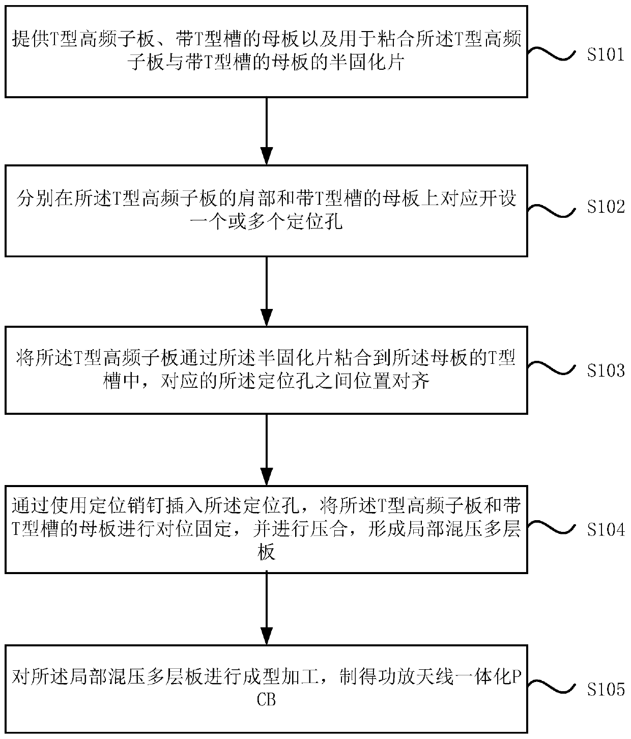
[0052] see figure 1 , the first embodiment provides a method for manufacturing a power amplifier antenna integrated PCB, including steps:

[0053] S101. Provide a T-shaped high-frequency sub-board, a motherboard with a T-shaped slot, and a prepreg for bonding the T-shaped high-frequency sub-board and the motherboard with a T-shaped slot.

[0054] Wherein, the shape of the T-shaped slot matches the shape of the T-shaped high-frequency sub-board.

[0055] Specifically, the step of providing the T-shaped high-frequency sub-board in step S101 further includes:

[0056] (1) providing a plurality of first core boards and prepregs, the material of the first core boards being the first material;

[0057] Wherein, the first material is a high-frequency plate with low loss and low dielectric constant, which can ensure low loss and high-quality transmission of antenna signals.

[0058] (2) Place the prepreg between every two first core boards and press them together to form the first-...

Embodiment 2

[0096] The second embodiment provides an integrated power amplifier and antenna PCB, which is manufactured according to the manufacturing method provided in the first embodiment.


PUM


Abstract

The embodiment of the invention discloses a fabrication method of a power amplifier antenna integrated PCB and the power amplifier antenna integrated PCB. The method comprises the steps of providing aT-shaped high-frequency sub-board, a mother board with a T-shaped groove and a prepreg, wherein the prepreg is used for pasting the T-shaped high-frequency sub-board and the mother board with the T-shaped groove; respectively and correspondingly forming one or more positioning holes in a shoulder part of the T-shaped high-frequency sub-board and the mother board with the T-shaped groove; pastingthe T-shaped high-frequency sub-board to the T-shaped groove of the mother board by the prepreg, and allowing positions among the corresponding positioning holes to be aligned; inserting positioning pins into the positioning holes, aligning and fixing the T-shaped high-frequency sub-board and the mother board with the T-shaped groove, performing lamination, and forming a local mix-pressed multi-layer board; and forming and processing the local mix-pressed multi-layer board to fabricate the power amplifier antenna integrated PCB. According to the method provided by the technical scheme of the embodiment of the invention, the fabrication cost of the whole board can be greatly reduced, the favorable reliability of a product is ensured, the alignment of a high-intensive blind hole in an outerlayer and the whole board also can be ensured, and favorable welding feasibility of a PCBA is ensured.

Description

technical field [0001] Embodiments of the present invention relate to the technical field of printed circuit boards, in particular to a method for manufacturing a power amplifier antenna integrated PCB and a power amplifier antenna integrated PCB. Background technique [0002] At present, the fifth-generation wireless mobile communication is developing rapidly. The difference between the new-generation antenna products and the traditional communication system products is that the power supply area and the antenna part of the new-generation antenna products are fitted into a unified whole and designed in the same printed circuit board. , which can improve the emission strength and transmission quality of the signal. Among the integrated power amplifier and antenna products currently designed in the industry, most of them use ultra-low loss, low dielectric constant boards, and the whole board is pressed together. This design has the following shortcomings: [0003] (1) The cu...

Claims


Application Information

Patent Timeline
Patent Type & Authority Applications(China)
IPC IPC(8): H05K3/46
Inventor 魏华李小东薛美贵
Owner DONGGUAN POLYTECHNIC
Why Eureka
Try Eureka