
Substrate for semiconductor device, semiconductor device, and method for manufacturing substrate for semiconductor device

A manufacturing method and semiconductor technology, applied in semiconductor/solid-state device manufacturing, semiconductor devices, transistors, etc., can solve problems such as current collapse, buffer layer crystallinity reduction, easy deterioration, etc., and achieve the effect of suppressing current collapse phenomenon

Active Publication Date: 2019-05-03
SANKEN ELECTRIC CO LTD +1
View PDF9 Cites 2 Cited by
  • Summary
  • Abstract
  • Description
  • Claims
  • Application Information

AI Technical Summary

Problems solved by technology

[0016] Furthermore, in order to solve the above-mentioned problems, although the leakage current in the lateral direction during high-temperature operation can be suppressed by making the buffer layer contain carbon, if the average concentration of carbon is increased too much, the crystallinity of the buffer layer will decrease, and the current collapse will occur. Problems that tend to worsen

Method used


Image

  • Substrate for semiconductor device, semiconductor device, and method for manufacturing substrate for semiconductor device
  • Substrate for semiconductor device, semiconductor device, and method for manufacturing substrate for semiconductor device
  • Substrate for semiconductor device, semiconductor device, and method for manufacturing substrate for semiconductor device

Examples


Embodiment

[0111] Hereinafter, although an Example is shown and this invention is demonstrated more concretely, this invention is not limited to this.

[0112] [Example]

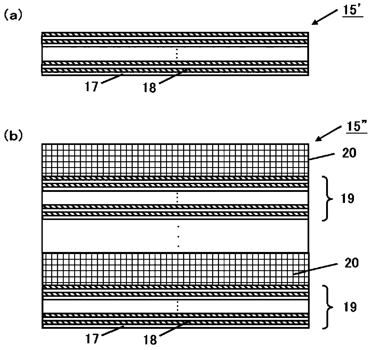
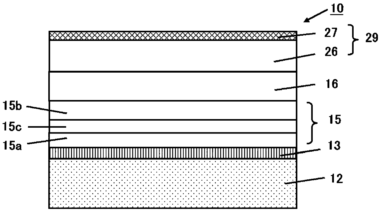
[0113] use for Figure 5 and Image 6 The method for manufacturing a substrate for a semiconductor device described above produces a substrate for a semiconductor device. However, as the initial layer, an initial layer 13 made of AlN is formed on the substrate 12, and an Fe-doped layer (iron concentration: 1×10 18 atoms / cm 3 above) as the first region 15a. The first area 15a is as figure 2 The laminate structure shown in (b) is a laminate structure in which eight pairs of AlN layers 17 and GaN layers 18 are laminated alternately, and six pairs of GaN insertion layers 20 are alternately laminated.

[0114] An undoped (undope) Fe layer (without introducing Cp) is formed on the first region 15a. 2 Layers formed of Fe: the third region 15c and the second region 15b). The carbon concentration of the upper layer (se...


PUM


Abstract

The present invention is a substrate for a semiconductor device having a substrate, a buffer layer which is provided on the substrate and which comprises a nitride semiconductor, and a device active layer comprising a nitride semiconductor layer provided on the buffer layer, wherein the substrate for a semiconductor device is characterized in that: the buffer layer has a first region containing carbon and iron, and a second region which is located on the first region and which has a lower average concentration of iron than does the first region and a higher average concentration of carbon thandoes the first region; and the average concentration of carbon in the second region is lower than the average concentration of iron in the first region. Thereby provided is a substrate for a semiconductor device with which it is possible to suppress a lateral leak current during high-temperature operation of the device while suppressing a longitudinal leak current, and to suppress a current collapse phenomenon.

Description

technical field [0001] The present invention relates to a substrate for a semiconductor device, a semiconductor device, and a method for manufacturing a substrate for a semiconductor device. Background technique [0002] A substrate for a semiconductor device using a nitride semiconductor is used for a power supply unit or the like that operates at high frequency and high output. In particular, it is particularly suitable for amplification in high-frequency regions such as microwaves, submillimeter waves, and millimeter waves. For example, high electron mobility transistors (High Electron Mobility Transistor, HEMT) and the like are known. [0003] A substrate for a semiconductor device using such a HEMT or the like is disclosed in Patent Document 1, for example. In Patent Document 1, a substrate for a semiconductor device such as Figure 12 As shown, there is: a buffer layer 114 formed on a silicon substrate 111 formed by alternating layers of a first semiconductor layer 11...

Claims


Application Information

Patent Timeline
Patent Type & Authority Applications(China)
IPC IPC(8): H01L21/338H01L21/20H01L21/205H01L29/778H01L29/812
CPCH01L21/02378H01L21/02381H01L21/02507H01L21/0254H01L21/02579H01L21/02581H01L21/0262H01L21/02458H01L29/7786H01L29/2003H01L29/1075H01L29/66462H01L29/778H01L29/812H01L29/7781
Inventor 佐藤宪鹿内洋志筱宫胜土屋庆太郎萩本和德
Owner SANKEN ELECTRIC CO LTD
Learn More