A mid-infrared band modulator and its preparation method

A technology of infrared band and modulator, which is applied in the field of mid-infrared band modulator and its preparation, can solve the problems of narrow optical bandwidth, etc., and achieve the effect of reducing thermal mismatch and being easy to realize

Active Publication Date: 2020-09-15
INST OF SEMICONDUCTORS - CHINESE ACAD OF SCI
View PDF6 Cites 0 Cited by
  • Summary
  • Abstract
  • Description
  • Claims
  • Application Information

AI Technical Summary

Problems solved by technology

In the prior art, GeSn has been used in detectors, but it is only in the theoretical design stage for modulators; another method is micro-ring resonant modulator (MRRM), and the optical bandwidth of MRRM is narrow

Method used


Image

  • A mid-infrared band modulator and its preparation method
  • A mid-infrared band modulator and its preparation method
  • A mid-infrared band modulator and its preparation method

Examples


Embodiment Construction

[0034] In order to make the purpose, technical solutions and advantages of the present disclosure clearer, the present disclosure will be further described in detail below in conjunction with specific embodiments and with reference to the accompanying drawings.

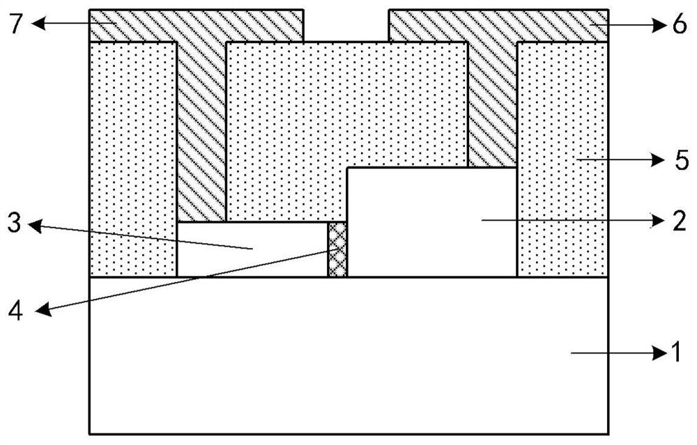
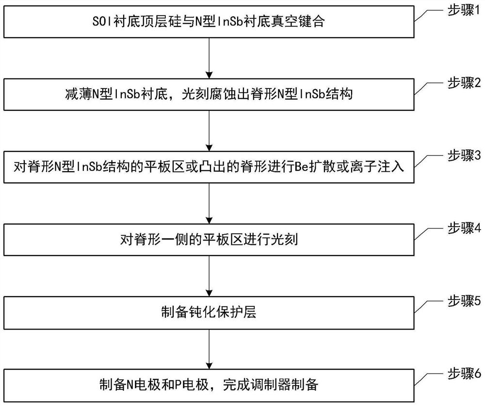
[0035] The disclosure provides a mid-infrared band modulator and a preparation method thereof. By bonding the N-type InSb substrate with Si material, the N-type InSb substrate is etched into a ridge waveguide, and the Or the ridge area protruding from the flat area is diffused or ion-implanted to form a P-type InSb structure, and the N-type InSb structure and the P-type InSb structure form a PN junction, and a narrow neutral region I region is formed in the middle of the PN junction. When the external mid-infrared light is input, the carrier concentration of this P(I)N structure InSb material changes with the increase of the applied voltage, and the refractive index and absorptivity increase accordingly, absorbing in t...


PUM

PropertyMeasurementUnit
thicknessaaaaaaaaaa
thicknessaaaaaaaaaa
widthaaaaaaaaaa

Abstract

The invention provides a mid-infrared band modulator preparation method. The method comprises the steps that 1, vacuum bonding is conducted on an SOI substrate top silicon (1) and an N-type InSb substrate (20); 2, the N-type InSb substrate (20) is thinned and then etched to obtain a ridge N-type InSb structure (2) which includes the ridge in the middle and flat areas on the two sides; 3, the flatareas are transformed into a P-type InSb structure (3), or the ridge protruding out of the flat areas is transformed into the P-type InSb structure (3), and meanwhile a neutral area I (4) is formed between the N-type InSb structure (2) and P-type InSb structure (3); 4, photoetching corrosion is conducted on the flat area on one side of the ridge, and the flat area on the other side of the ridge isretained; 5, a passive protective layer (5) is prepared; 6, an N electrode (6) and a P electrode (7) are prepared. The invention further provides a mid-infrared band modulator.

Description

technical field [0001] The present disclosure relates to the technical field of semiconductor devices, in particular to a mid-infrared band modulator and a preparation method thereof. Background technique [0002] Mid-infrared (mid-IR) wavelengths are an important area of ​​silicon photonics not only for sensing applications but also as parallel communication windows for communication infrastructure. When communication approaches the theoretical capacity limit of traditional single-mode fiber (SMF), hollow-core photonic bandgap fiber (HC-PBGF) has lower predicted loss and nonlinearity compared with the best single-mode fiber, and its lowest loss Calculated values ​​are around the mid-infrared, which opens up a new band for communications. Milos and Soref pointed out that the 1-14μm band covers the basic absorption characteristics of many important chemical and biomolecules. The analysis of the refractive index and absorption coefficient in this band can extend our applicati...

Claims


Application Information

Patent Timeline
Patent Type & Authority Patents(China)
IPC IPC(8): G02F1/015
CPCG02F1/015G02F1/0151G02F1/0155
Inventor 郑婉华彭红玲马丕杰董凤鑫石涛齐爱谊
Owner INST OF SEMICONDUCTORS - CHINESE ACAD OF SCI
Why Eureka
Try Eureka