Polycrystalline silicon ingot and polycrystalline silicon rod prepared from silicon materials purified according to physical method, and methods thereof

A technology of polycrystalline silicon ingots and polycrystalline silicon rods is applied in the field of semiconductors, which can solve the problems of high impurities in silicon materials, low performance of silicon wafers, restricting the price of solar cells, etc., and achieve the effects of reducing costs and improving performance.

Inactive Publication Date: 2019-04-05
ZHEJIANG JINKO SOLAR CO LTD +1
View PDF6 Cites 0 Cited by
  • Summary
  • Abstract
  • Description
  • Claims
  • Application Information

AI Technical Summary

Problems solved by technology

Most of the silicon materials used in the solar energy industry are chemical methods. The silicon materials purified by the Siemens method can reach a purity of 6N-7N. However, the cost of chemically purified silicon materials is relatively high, which restricts the price of solar cells.
Although the silicon material purified by physical method is relatively low in cost, its purity can only reach 4N-5N. The silicon material has many impurities and the impurities are mainly Al, Fe, Ti, Ca, B, P, etc. Silicon ingots prepared by ingot casting, crystal pulling process and physical purification of silicon materials, the metal impurities and non-metallic (B, P, etc.) impurities in it will lead to low performance of silicon wafers made from this silicon ingot

Method used


Image

  • Polycrystalline silicon ingot and polycrystalline silicon rod prepared from silicon materials purified according to physical method, and methods thereof
  • Polycrystalline silicon ingot and polycrystalline silicon rod prepared from silicon materials purified according to physical method, and methods thereof

Examples


Embodiment Construction

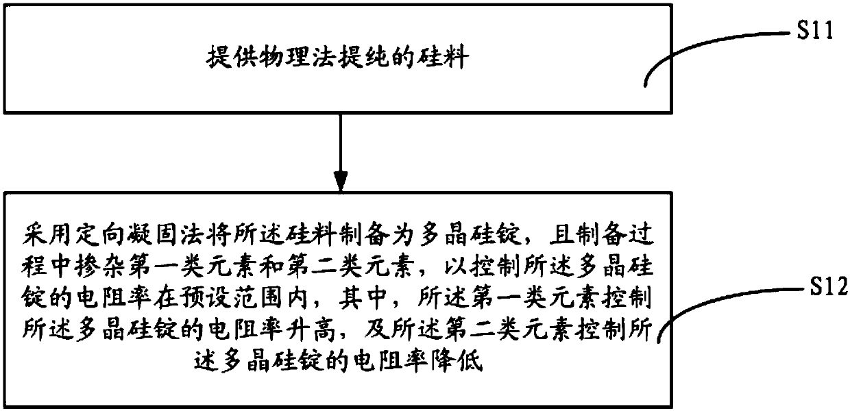
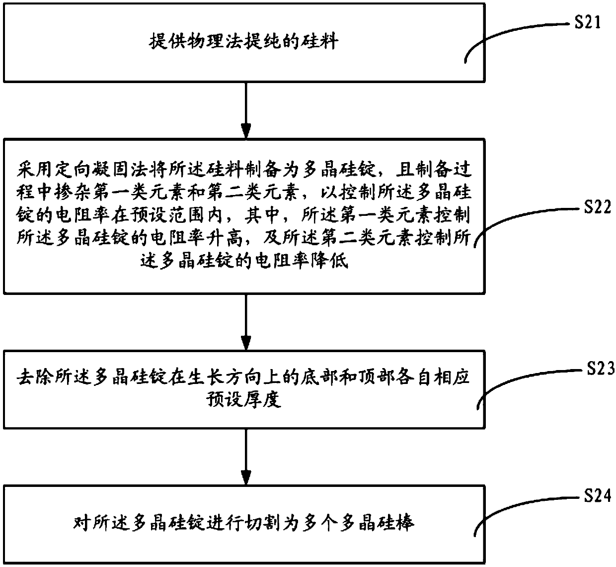
[0030] The following will clearly and completely describe the technical solutions in the embodiments of the present invention with reference to the accompanying drawings in the embodiments of the present invention. Obviously, the described embodiments are only some, not all, embodiments of the present invention. Based on the embodiments of the present invention, all other embodiments obtained by persons of ordinary skill in the art without making creative efforts belong to the protection scope of the present invention.

[0031] As mentioned in the background technology, with the maturity of the photovoltaic market, the increasingly fierce competition, and the rapid expansion of the industry's development volume, it is a good idea to reduce the cost of photovoltaic production by reducing the cost of raw materials under the premise that the existing technology cannot make breakthroughs quickly. The most effective method, such as reducing the cost of polysilicon materials. Most o...


PUM


Abstract

The invention discloses a polycrystalline silicon ingot and a polycrystalline silicon rod prepared from silicon materials purified according to a physical method, and corresponding methods thereof. The silicon materials are prepared into the polycrystalline silicon ingot according to a directional solidification method; a first-type element and a second-type element are doped in the preparation process to control the resistivity of the polycrystalline silicon ingot within a preset range, wherein the first-type element controls the resistivity increase of the polycrystalline silicon ingot, andthe second-type element controls the resistivity reduction of the polycrystalline silicon ingot. According to the technical scheme, the polycrystalline silicon ingot is prepared by the directional solidification method to remove metal impurities, and accordingly, the metal impurities in the polycrystalline silicon ingot and the polycrystalline silicon rod can be removed effectively; through dopingof the first-type element and the second-type element, the doping balance in the polycrystalline silicon ingot and the polycrystalline silicon rod can be realized to control the resistivity within the preset range, so that the performance of silicon wafers prepared from the polycrystalline silicon ingot or the polycrystalline silicon rod is improved, and the cost of semiconductor structural devices is effectively reduced.

Description

technical field [0001] The invention relates to the technical field of semiconductors, more specifically, to a polycrystalline silicon ingot and a polycrystalline silicon rod prepared from silicon material purified by a physical method and a corresponding method. Background technique [0002] As the photovoltaic market matures, the competition becomes increasingly fierce, and the development volume of the industry rapidly expands. Under the premise that existing technologies cannot make rapid breakthroughs, it is an effective method to reduce the cost of photovoltaic production by reducing the cost of raw materials. For example, Reduce the cost of polysilicon material. Most of the silicon materials used in the solar energy industry are chemical methods. The silicon materials purified by the Siemens method can reach a purity of 6N-7N. However, the cost of chemically purified silicon materials is relatively high, which restricts the price of solar cells. Although the silicon ...

Claims


Application Information

Patent Timeline
Patent Type & Authority Applications(China)
IPC IPC(8): C30B29/06C30B28/06
CPCC30B28/06C30B29/06
Inventor 闫灯周刘俊辉郭志球
Owner ZHEJIANG JINKO SOLAR CO LTD
Why Eureka
Try Eureka