


Quick Research
Generate reliable direction feasibility study reports for your R&D in just a few steps.

Technical Q&A
Discover and master advanced knowledge NOW. Basics, ideas, possibilities, all at once.

Find Solutions
As an expert in R&D theories, this can generate solutions to your technical problems instantly.

Evaluate Feasibility
Analyze your overall solution with one click, know your potential R&D risks in advance.

Monitor Landscape
Get weekly tech updates, stay abreast of the latest tech innovations and key insights.
A method for preparing an inverted octagonal pyramid-shaped patterned silicon substrate
A patterned, silicon substrate technology, applied in the direction of final product manufacturing, sustainable manufacturing/processing, climate sustainability, etc., can solve the problems of inability to prepare pyramids, and difficult to etch pyramid-shaped patterned silicon substrates, and achieve excellent results. Light trapping ability, the effect of reducing reflectivity, increasing optical path length
- Summary
- Abstract
- Description
- Claims
- Application Information
AI Technical Summary
Problems solved by technology
Method used
Image


Examples
specific Embodiment approach 1
[0020] Specific Embodiment 1: In this embodiment, a method for preparing an inverted octagonal truss-shaped patterned silicon substrate is carried out according to the following steps:
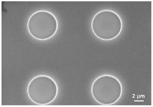
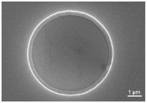
[0021] 1. Preparation of silicon dioxide mask: using a photolithography process to prepare a circular hole-shaped silicon dioxide mask on a single crystal silicon substrate to obtain a silicon wafer covered with a circular hole-shaped silicon dioxide mask;
[0022] 2. Wet etching: place the silicon wafer covered with a round-hole silicon dioxide mask on a polytetrafluoroethylene flower basket and suspend it in the TMAH solution, then heat the TMAH solution to 25-80°C, and then etch , to obtain the etched silicon wafer;
[0023] 3. Removing the silicon dioxide mask: Take the PTFE flower basket containing the etched silicon wafer out of the TMAH solution and rinse it with deionized water, then place it in the BOE solution for etching for 2-5 minutes, and then rinse it with deionized water And b...
specific Embodiment approach 2
[0031] Embodiment 2: This embodiment differs from Embodiment 1 in that the silicon dioxide mask with circular holes in step 1 is a periodic silicon dioxide mask with circular holes. Others are the same as in the first embodiment.
specific Embodiment approach 3
[0032] Embodiment 3: The difference between this embodiment and Embodiment 1 or 2 is that the concentration of the TMAH solution in step 2 is 1wt%-4wt%, and the etching is 1-8min. Others are the same as in the first or second embodiment.
PUM
| Property | Measurement | Unit |
|---|---|---|
| thickness | aaaaa | aaaaa |
| pore size | aaaaa | aaaaa |
Abstract
Description
Claims
Application Information
 - R&D Engineer
- R&D Manager
- IP Professional
- Industry Leading Data Capabilities
- Powerful AI technology
- Patent DNA Extraction
Browse by: Latest US Patents, China's latest patents, Technical Efficacy Thesaurus, Application Domain, Technology Topic, Popular Technical Reports.
© 2024 PatSnap. All rights reserved.Legal|Privacy policy|Modern Slavery Act Transparency Statement|Sitemap|About US| Contact US: help@patsnap.com