


Quick Research
Generate reliable direction feasibility study reports for your R&D in just a few steps.

Technical Q&A
Discover and master advanced knowledge NOW. Basics, ideas, possibilities, all at once.

Find Solutions
As an expert in R&D theories, this can generate solutions to your technical problems instantly.

Evaluate Feasibility
Analyze your overall solution with one click, know your potential R&D risks in advance.

Monitor Landscape
Get weekly tech updates, stay abreast of the latest tech innovations and key insights.
A process method for composite asynchronous polishing of ceramics by picosecond-nanosecond laser
一种皮秒激光、工艺方法的技术,应用在激光焊接设备、制造工具、金属加工设备等方向,能够解决材料去除量多、表面形貌易破坏、热/机械应力影响区大等问题,达到熔点低、表面活性大的效果
- Summary
- Abstract
- Description
- Claims
- Application Information
AI Technical Summary
Problems solved by technology
Method used
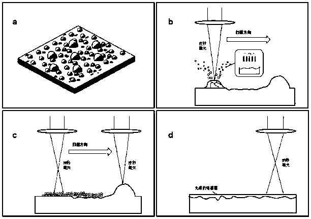
Image


Examples
Embodiment 1
[0023] To polish the 95% alumina ceramic substrate, first use the picosecond laser with an average power of 60W, a repetition rate of 100,000KHz, and a defocus of 0 to start scanning irradiation, with a scanning speed of 400mm / s and a scanning path gap of 0.05mm. Sputtering used to remove material microscopic surface protrusions and excite micro-nano particles. After 50μs, the average power is 5W, the repetition frequency is 100KHz, and the nanosecond laser with a defocus of +0.3mm tracks the picosecond laser scanning path to irradiate at the same speed, which is used to melt the micro-nano particles produced by picosecond laser irradiation. It produces a layer of uniform and dense fine-grained fused layer. The used polishing process was taken out from the processing platform, and the surface microscopic appearance was tested by laser confocal microscope. The roughness Ra decreased from the original 1.70 μm to 0.68 μm. The three-dimensional appearance of the surface before and...
Embodiment 2
[0025] To polish the zirconia ceramic substrate, first use a picosecond laser with an average power of 30W, a repetition rate of 50,000KHz, and a defocus of 0 to start scanning irradiation. The scanning speed is 1000mm / s, and the scanning path gap is 0.01mm. , for sputtering to remove material microscopic surface protrusions and excite micro-nano particles. After 50μs, start the nanosecond laser with an average power of 3W, a repetition rate of 50KHz, and a defocus of +0.5mm to track the picosecond laser scanning path to irradiate at the same speed, which is used to melt the micro-nano particles produced by picosecond laser irradiation, so that It produces a uniform dense fine-grained fused layer. The used polishing process was taken out from the processing platform, and the surface micro-morphology was tested using a laser confocal microscope. The roughness Ra decreased from the original 1.30 μm to 0.52 μm. The three-dimensional surface morphology before and after polishing i...
Embodiment 3
[0027]To polish the aluminum nitride ceramic substrate, first use a picosecond laser with an average power of 55W, a repetition rate of 100,000KHz, and a defocus of 0 to start scanning irradiation, with a scanning speed of 300mm / s and a scanning path gap of 0.5mm. Sputtering used to remove material microscopic surface protrusions and excite micro-nano particles. After 100μs, the average power is 14W, the repetition frequency is 100KHz, and the nanosecond laser tracking picosecond laser scanning path is irradiated at the same speed with a defocus of +0.1mm, which is used to melt the micro-nano particles produced by picosecond laser irradiation, so that It produces a uniform dense fine-grained fused layer. The used polishing process was taken out from the processing platform, and the surface micromorphology was tested using a laser confocal microscope. The roughness Ra dropped from the original 1.81 μm to 0.65 μm.
PUM
| Property | Measurement | Unit |
|---|---|---|
| power | aaaaa | aaaaa |
| power | aaaaa | aaaaa |
| Defocus amount | aaaaa | aaaaa |
Abstract
Description
Claims
Application Information
 - R&D Engineer
- R&D Manager
- IP Professional
- Industry Leading Data Capabilities
- Powerful AI technology
- Patent DNA Extraction
Browse by: Latest US Patents, China's latest patents, Technical Efficacy Thesaurus, Application Domain, Technology Topic, Popular Technical Reports.
© 2024 PatSnap. All rights reserved.Legal|Privacy policy|Modern Slavery Act Transparency Statement|Sitemap|About US| Contact US: help@patsnap.com