Isolator based on magneto-optic waveguide and preparation method thereof
An optical isolator and isolator technology, applied in the field of integrated preparation and miniaturization, can solve the problems of large size of the isolator and cannot meet the requirements of miniaturization and integration, and achieve the effect of miniaturization and size reduction
- Summary
- Abstract
- Description
- Claims
- Application Information
AI Technical Summary
Problems solved by technology
Method used
Image
Examples
Embodiment 1
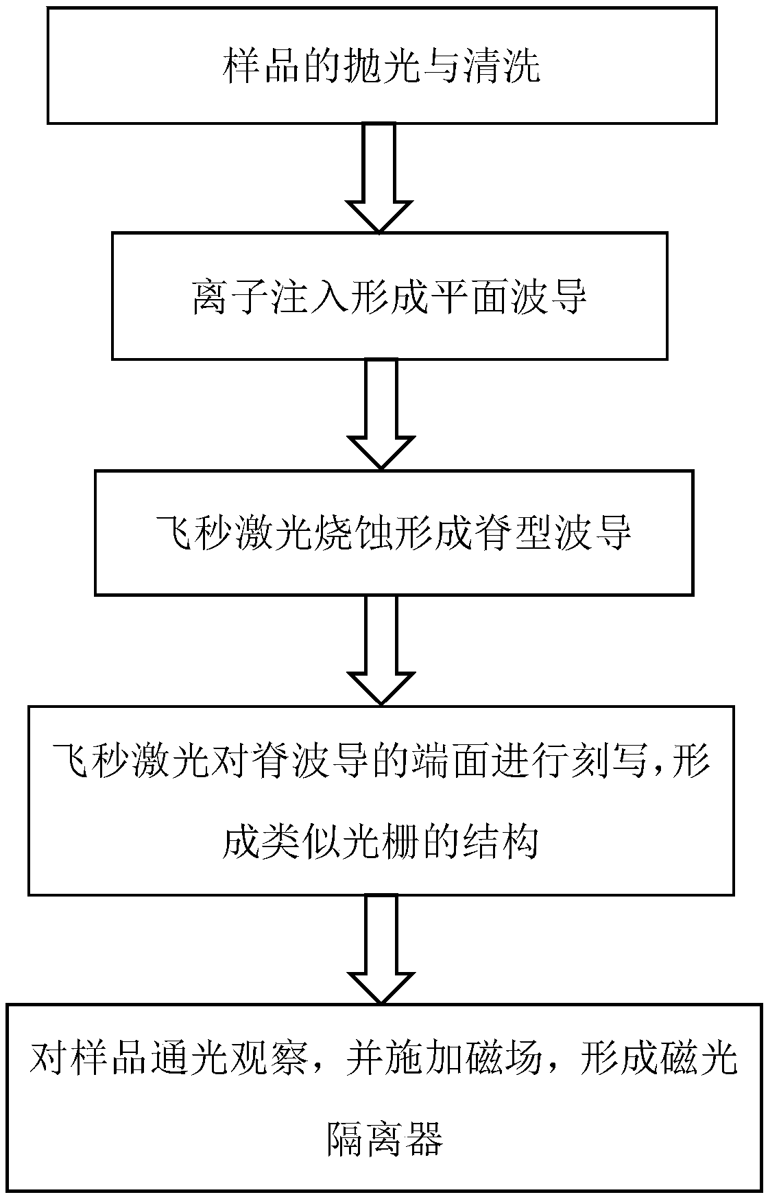
[0033] 1) Sample treatment: cut the magneto-optical glass sample into a size of 10.0mm×10.0mm×1.0mm, and perform optical polishing on the surface and end surface of the sample. The polished sample was first ultrasonicated with acetone for 20 minutes, and then cleaned with ethanol and deionized water respectively;
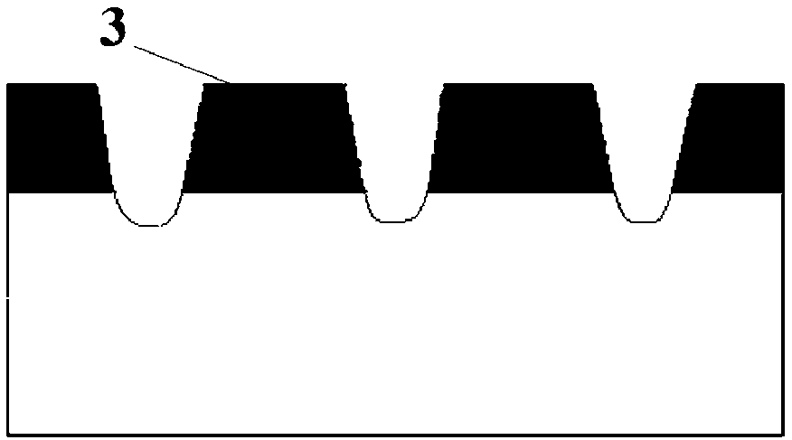
[0034] 2) Preparation of a planar waveguide structure: put the sample treated in step 1) into a 2×1.7MV tandem accelerator, inject energy at 550keV, and dose 4.0×10 16 ions / cm 2 of hydrogen ions. Hydrogen ions implanted into magneto-optical glass form a planar waveguide such as image 3 shown. Clean the planar optical waveguide successively with acetone, ethanol, and deionized water.
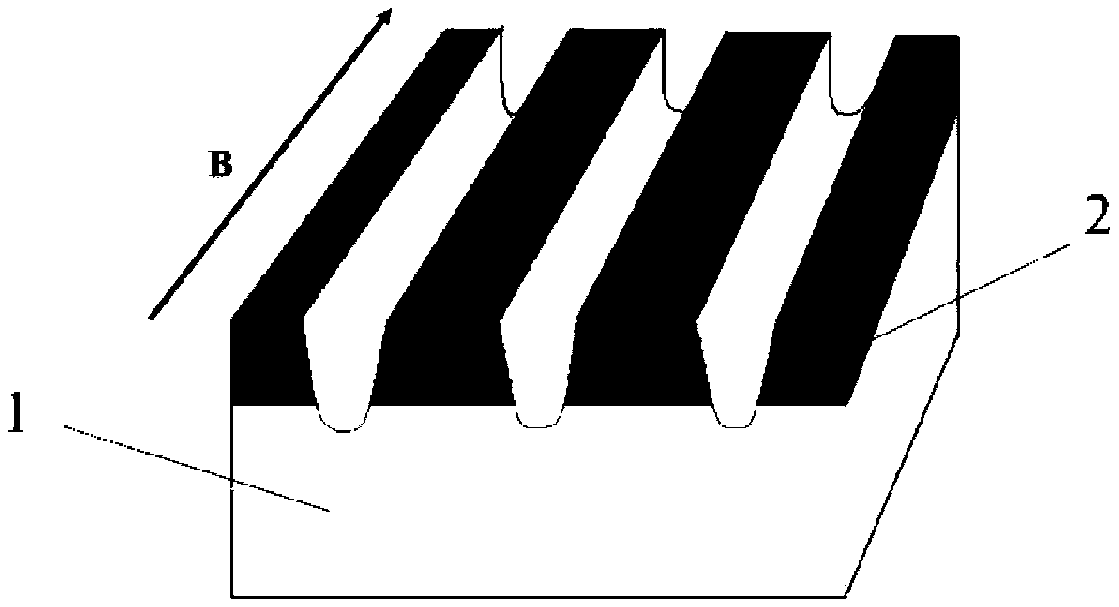
[0035] 3) Preparation of the ridge waveguide structure: the cleaned planar optical waveguide structure is placed on a three-dimensional adjustment platform with a spatial resolution of 0.2 μm. Use a Ti:Sapphire laser system with a wavelength of 800 nm, a pulse width of 220 fs, an...
Embodiment 2
[0039] 1) Sample treatment: cut the magneto-optical glass sample into a size of 10.0mm×10.0mm×1.0mm, and perform optical polishing on the surface and end surface of the sample. The polished sample was first ultrasonicated with acetone for 20 minutes, and then cleaned with ethanol and deionized water respectively;
[0040] 2) Preparation of planar waveguide structure: put the sample treated in step 1) into a 2×1.7MV tandem accelerator, inject energy at 6MeV, and dose at 2.0×10 15 ions / cm 2 of silicon ions. Silicon ions implanted into magneto-optical glass to form a planar optical waveguide such as image 3 shown. Clean the planar optical waveguide successively with acetone, ethanol, and deionized water.
[0041] 3) Preparation of a ridge waveguide structure: the cleaned planar optical waveguide is placed on a three-dimensional adjustment platform with a spatial resolution of 0.2 μm. Use a Ti:Sapphire laser system with a wavelength of 800 nm, a pulse width of 220 fs, and a ...
PUM
 Abstract
Description
Claims
Application Information
 - R&D
- Intellectual Property
- Life Sciences
- Materials
- Tech Scout
- Unparalleled Data Quality
- Higher Quality Content
- 60% Fewer Hallucinations
Browse by: Latest US Patents, China's latest patents, Technical Efficacy Thesaurus, Application Domain, Technology Topic, Popular Technical Reports.
© 2025 PatSnap. All rights reserved.Legal|Privacy policy|Modern Slavery Act Transparency Statement|Sitemap|About US| Contact US: help@patsnap.com


