Rework process and method for sapphire single-sided polished section thickness badness
A technology for single-sided polishing and sapphire wafers, applied to surface polishing machine tools, grinding/polishing equipment, manufacturing tools, etc.
- Summary
- Abstract
- Description
- Claims
- Application Information
AI Technical Summary
Problems solved by technology
Method used
Image

Examples
Embodiment Construction
[0014] specific implementation plan
[0015] Below in conjunction with accompanying drawing, the embodiment of the present invention is described:
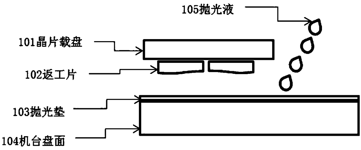
[0016] Basic sapphire single-sided polished wafers with poor thickness rework steps: First, survey and map the polished sapphire wafers with poor thickness; through surveying and mapping analysis, the areas with poor inner and outer rings on the surface of the sapphire wafer thickness (TTV, LTV, TIR, pits); according to The numerical analysis of the poor surface thickness of the sapphire wafer combined with the principle of the maximum utilization of the wafer trims the surface of the polishing disk; finally, the adjusted polishing disk is used to face the sapphire wafer for single-sided polishing. After polishing, it is washed and dried with high temperature acid and alkali, and finally the polishing is measured. After the thickness of the sapphire wafer (TTV, LTV, TIR, pits), until the flatness requirements are met, a nano-scale...
PUM
 Abstract
Description
Claims
Application Information
 - Generate Ideas
- Intellectual Property
- Life Sciences
- Materials
- Tech Scout
- Unparalleled Data Quality
- Higher Quality Content
- 60% Fewer Hallucinations
Browse by: Latest US Patents, China's latest patents, Technical Efficacy Thesaurus, Application Domain, Technology Topic, Popular Technical Reports.
© 2025 PatSnap. All rights reserved.Legal|Privacy policy|Modern Slavery Act Transparency Statement|Sitemap|About US| Contact US: help@patsnap.com