Design method for cathode short MOS-controlled thyristor layout

A layout design, thyristor technology, applied in circuits, electrical components, electrical solid devices, etc., can solve the problems of burnt devices, enhanced gate signal delay effect, heat accumulation, etc., to shorten the time difference of latch, uniform current distribution, reduce The effect of heat accumulation

Inactive Publication Date: 2019-02-05
UNIV OF ELECTRONICS SCI & TECH OF CHINA
View PDF7 Cites 2 Cited by
  • Summary
  • Abstract
  • Description
  • Claims
  • Application Information

AI Technical Summary

Problems solved by technology

However, the device works under pulse conditions, and the carriers cannot diffuse in time in a short period of time, and under the positive feedback mechanism, the current of the cells that are preferentially latched continues to increase, resulting in excessive current concentrated and distributed on the edge of the preferentially triggered latch. At the inflection point of the cathode of the cell, local heat accumulation is formed here, so that the device is burned; secondly, as the internal gate resistance increases, the delay effect of the internal cell on the gate signal is enhanced, and the moment when the internal cell triggers the latch gradually Delay will further intensify the non-simultaneous triggering effect of edge cells and internal cells
When the internal gate resistance reaches a certain value and the resistance of the edge cells of the leading latch is very small, the internal cells have not yet triggered the latch, and all the current will flow into the low-resistance edge cells, resulting in extremely uneven current distribution, thus Faster burning of edge cells

Method used


Image

  • Design method for cathode short MOS-controlled thyristor layout
  • Design method for cathode short MOS-controlled thyristor layout
  • Design method for cathode short MOS-controlled thyristor layout

Examples


Embodiment

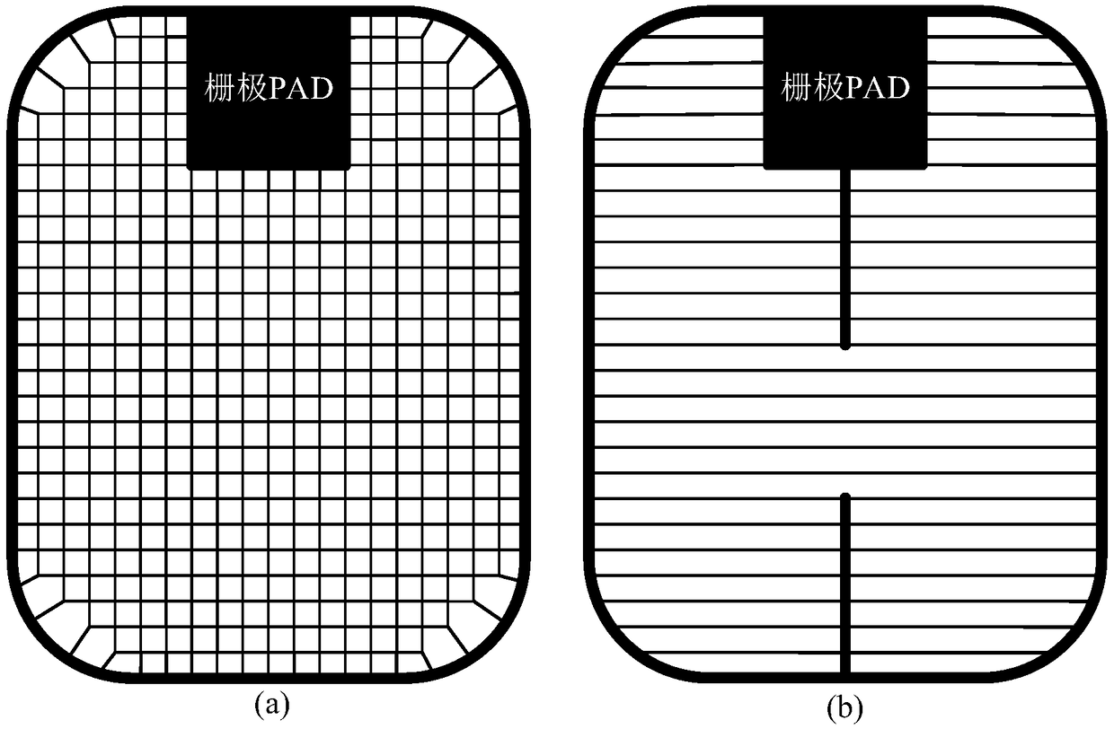
[0029] Taking a device with a cell width of 50 μm as an example, the withstand voltage is 1700V. Figure 4Schematic diagram of the topological circuit for the CS-MCT device under transient simulation. Among them, the device works in the RLC loop, the capacitance C is 0.72μF, the charge is 1100V, the inductance L A and L C Both are 20nH, R gex is 5Ω, the gate voltage is 10V, change R gin The value of the gate parasitic resistance at the time of failure is used as the benchmark for normalization processing, and the discharge situation of the CS-MCT device under the high current pulse is obtained. Taking this as an example, it is intuitively shown that the layout design of the present invention is different from the conventional CS-MCT device. The layout design of MCT has the performance advantage in this application field.

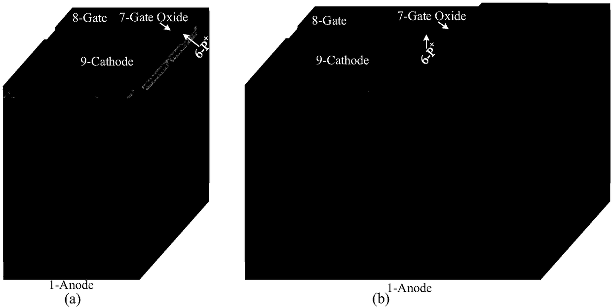
[0030] Compared Figure 5 with Image 6 In the figure, the distribution of the anode current in the internal cell and the edge cell during the pulse d...


PUM


Abstract

The invention belongs to the technical field of power semiconductor devices, and relates to a design method for a cathode short MOS-controlled thyristor (CS-MCT) layout. The method main includes forming a cellular grid structure into a bar-shaped grid structure in a horizontal direction; and defining a circle of cells connected to a junction terminal as edge cells, and defining other cells as internal cells, wherein the semiconductor doping regions of the edge cells are connected to a cathode through a bar-shaped contact hole, and the internal cells are connected to the cathode through a square-shaped contact hole. The latching current of the edge cells can be increased through improved measurements, and the time of the edge cells entering a latch can be prolonged; gate capacitance can bereduced, and the time of internal cells entering the latch can be advanced; in the middle part of the horizontal direction, bar-shaped grids also have metal interdigital in a vertical direction, so that the gate resistance parasitized on polysilicon can be reduced, and the time of the internal cells entering the latch can be advanced as well; and in a word, current can be uniformly distributed bymaking the edge cells and the internal cells simultaneously trigger the latch.

Description

technical field [0001] The invention belongs to the technical field of power semiconductor devices, and relates to a layout design method of a cathode short-circuit gate-controlled thyristor (CS-MCT). Background technique [0002] With the upgrading of fuze systems in national defense and military defense, pulse power technology has developed rapidly. In addition, in food processing, medical treatment, waste water treatment, waste gas treatment, ozone preparation, generator ignition, ion implantation, material processing and other civilian fields, pulse power technology is also widely used. (Yu Mingwei. Design of LCC resonant pulse current source [D]. Harbin Institute of Technology, 2015.) The pulse power switch plays a pivotal role as a key device of pulse power supply. [0003] Currently, commonly used semiconductor pulse power switches include thyristors (SCRs), insulated gate bipolar transistors (IGBTs), and MOS-controlled thyristors (MCTs). The above-mentioned semicon...

Claims


Application Information

Patent Timeline
Patent Type & Authority Applications(China)
IPC IPC(8): H01L27/02
CPCH01L27/0211
Inventor 陈万军左慧玲刘超刘亚伟邓操
Owner UNIV OF ELECTRONICS SCI & TECH OF CHINA
Why Eureka
Try Eureka