Manufacturing method of oled panel, temporary pairing structure

A manufacturing method and panel technology, applied in the field of OLED manufacturing, can solve problems such as inability to meet demand

Active Publication Date: 2020-10-23
SEEYA OPTRONICS LTD
View PDF8 Cites 0 Cited by
  • Summary
  • Abstract
  • Description
  • Claims
  • Application Information

AI Technical Summary

Problems solved by technology

[0006] The magnetic adsorption method is only suitable for metal shadow masks. For shadow masks made of other materials (such as non-metallic materials), the existing magnetic adsorption method can no longer meet the demand

Method used


Image

  • Manufacturing method of oled panel, temporary pairing structure
  • Manufacturing method of oled panel, temporary pairing structure
  • Manufacturing method of oled panel, temporary pairing structure

Examples


Embodiment Construction

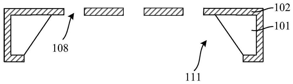
[0042] As mentioned in the background art, the magnetic adsorption method is only applicable to metal shadow masks. For shadow masks made of other materials (such as non-metallic materials), the existing magnetic adsorption method cannot meet the demand.

[0043] To this end, the present invention provides a method for manufacturing an OLED panel and a temporary pairing structure, wherein the method for manufacturing an OLED panel comprises sequentially combining the substrate with the first vapor deposition shadow mask, the second vapor deposition shadow mask or the third vapor deposition shadow mask. When the shadow mask is bonded and debonded three times, each bonding only requires the substrate on the outside of one of the corresponding bank structures (the first bank structure, the second bank structure or the third bank structure) UV glue is formed between the corresponding evaporation shadow masks, specifically when bonding for the first time (when forming the first ligh...


PUM

PropertyMeasurementUnit
wavelengthaaaaaaaaaa
thicknessaaaaaaaaaa
thicknessaaaaaaaaaa

Abstract

A method for manufacturing an OLED panel and a temporary pairing structure, the temporary pairing structure comprising: a substrate, a number of alternately distributed first dam structures and second dam structures located on the partial surface of the dam region of the substrate and surrounding the pixel region The weir structure and the third cofferdam structure; the vapor deposition shadow mask, including: a substrate; a grid film layer on the front surface of the substrate, and the grid film layer has a plurality of openings arranged in an array; located in the substrate and penetrating the substrate The thickness of the groove, the groove exposes some openings in the grid film layer and the grid film layer between adjacent openings; the substrate is inverted on the front side of the evaporation shadow mask, so that the cofferdam structure on the substrate Plating shadow mask contact; the UV glue formed between the substrate and the evaporation shadow mask outside one of the first cofferdam structure, the second cofferdam structure and the third cofferdam structure, the UV glue makes the substrate and the third cofferdam structure Evaporation shadow masks are bonded together. The structure of the invention improves the production efficiency of the OLED panel.

Description

technical field [0001] The invention relates to the field of OLED production, in particular to a production method and a temporary pairing structure of an OLED panel. Background technique [0002] Organic light-emitting diode (Organic Light-Emitting Diode, OLED) display panel also has self-illumination (no backlight required), high contrast, thin thickness, wide viewing angle, fast response, can be used for flexible panels, and has a wide temperature range Guanghe's structure and manufacturing process are relatively simple, and it is more and more favored by the industry. [0003] The original color scheme of the OLED display panel is to make a display unit that displays white light, and then use the corresponding color filter together. This technical solution This technical solution requires the introduction of color filters. Due to the blocking of color filters, about 80% of the light output from the display sub-pixels is lost in the color filters, which makes the light-e...

Claims


Application Information

Patent Timeline
Patent Type & Authority Patents(China)
IPC IPC(8): H01L27/32H01L51/00H01L51/56H01L21/68C23C14/04
CPCH01L21/682C23C14/042H10K59/122H10K71/166H10K71/00
Inventor 孔杰居宇涵
Owner SEEYA OPTRONICS LTD
Why Eureka
Try Eureka