
Semiconductor avalanche failure analyzing and testing method and device based on thermal imaging technology

A thermal imaging technology and failure analysis technology, which is applied in the field of robustness of power semiconductors and can solve the problem of not being able to observe the transfer of hot spots inside the device.

Active Publication Date: 2019-01-15
SOUTHEAST UNIV
View PDF9 Cites 4 Cited by
  • Summary
  • Abstract
  • Description
  • Claims
  • Application Information

AI Technical Summary

Problems solved by technology

[0004] At present, the widely used method for testing the avalanche failure of power devices is to put the power devices in the inductive circuit to form a traditional avalanche withstand test circuit. The avalanche breakdown of the device during this process is used to release the energy stored in the inductive load. This method releases a large amount of energy in a short time, calculates the avalanche withstand capacity of the device through the waveform, and judges the breakdown of the device through the breakdown position after the device is damaged. Weak points, but this method can only observe the final breakdown point of the device, but cannot observe the transfer of the internal heating point of the device before failure

Method used


Image

  • Semiconductor avalanche failure analyzing and testing method and device based on thermal imaging technology
  • Semiconductor avalanche failure analyzing and testing method and device based on thermal imaging technology
  • Semiconductor avalanche failure analyzing and testing method and device based on thermal imaging technology

Examples


Embodiment 1

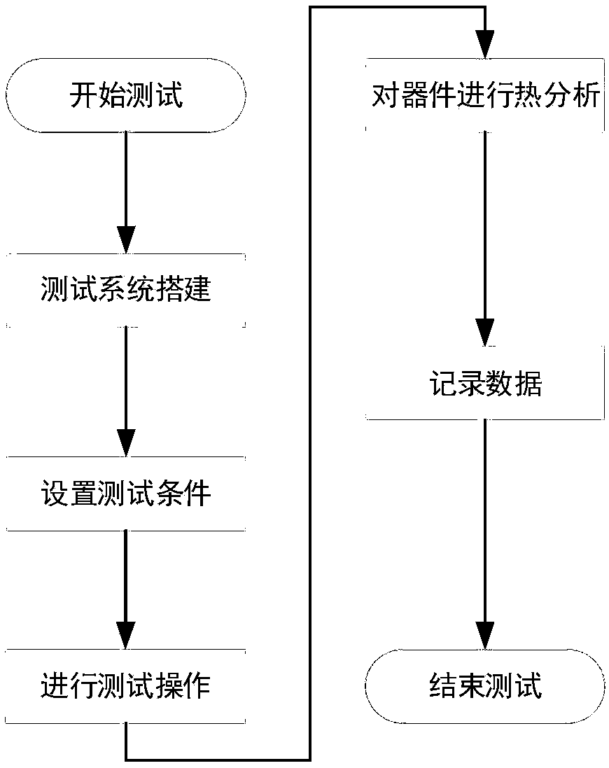
[0024] A test method for semiconductor avalanche failure analysis based on thermal imaging technology, comprising the following test steps:

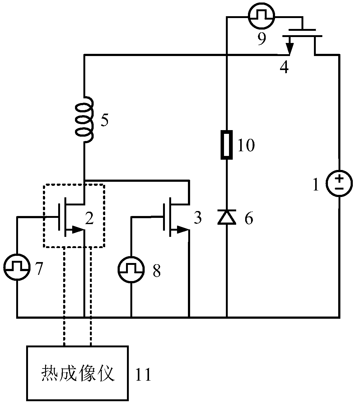
[0025] a) Test system construction: the system includes a DC voltage source 1 and a thermal imager 11, the positive pole of the DC voltage source 1 is connected to a power switching device 4 and is connected to the drain of the power switching device 4, and the negative pole of the DC voltage source 1 is connected There are a power device 2 to be tested, a short-circuit power device 3 and a freewheeling diode 6, and the negative pole of the DC voltage source 1 is connected to the source of the power device 2 to be tested, the source of the short-circuited power device 3 and the anode of the freewheeling diode 6 , the cathode of the freewheeling diode 6 is connected to a power resistor 10 and is connected to one end of the power resistor 10, and the other end of the power resistor 10 is connected to the grid of the power switching device 4...

Embodiment 2

[0031] A semiconductor avalanche failure analysis and testing device based on thermal imaging technology, including a DC voltage source 1 and a thermal imager 11, the anode of the DC voltage source 1 is connected to a power switching device 4 and connected to the drain of the power switching device 4, and the DC The negative pole of the voltage source 1 is connected to the power device 2 to be tested, the short-circuit power device 3 and the freewheeling diode 6, and the negative pole of the DC voltage source 1 is connected to the source of the power device 2 to be tested, the source of the short-circuit power device 3 and the freewheeling diode 6. The anode of the freewheeling diode 6 is connected, the cathode of the freewheeling diode 6 is connected with a power resistor 10 and connected with one end of the power resistor 10, and the other end of the power resistor 10 is connected to the gate of the power switching device 4 through the third pulse voltage source 9, to be The ...


PUM


Abstract

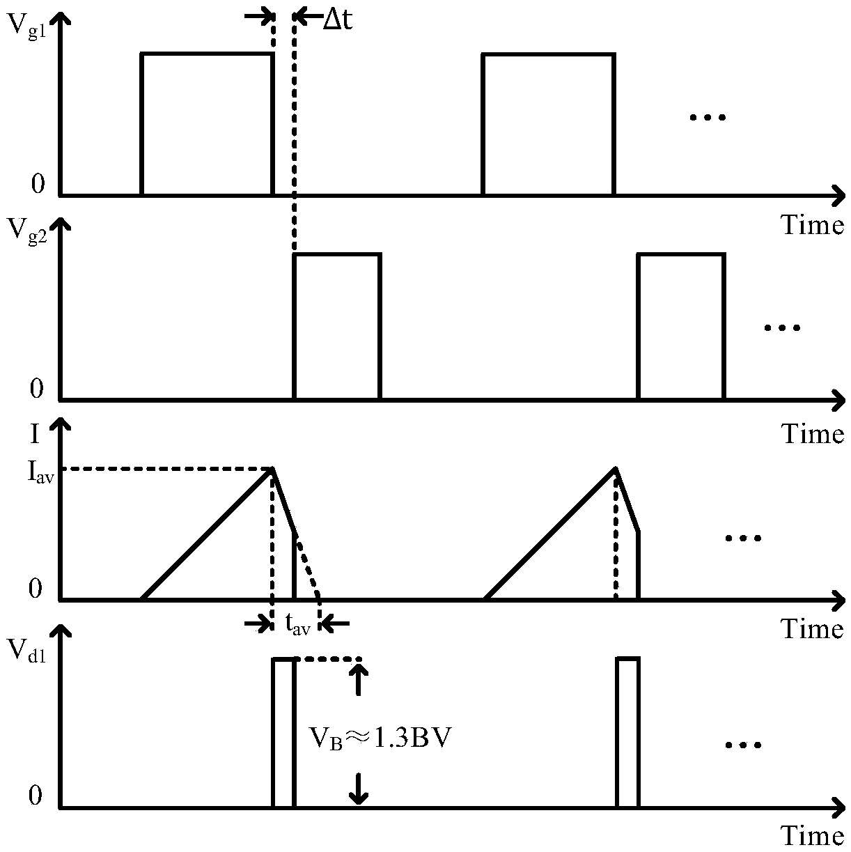
Disclosed is a semiconductor avalanche tolerance failure analyzing and testing method and device based on a thermal imaging technology. The semiconductor avalanche tolerance failure analyzing and testing method based on the thermal imaging technology mainly includes that, in a constructed test system, a to-be-tested power device and a power switch tube are turned on, an inductor starts to stream,the to-be-tested power device and the power switch tube are turned off after a current in the inductor reaches an avalanche current peak value Iav, the inductor discharges, and avalanche occurs in theto-be-tested power device, a short-circuit power device is turned on before the to-be-tested power device is broken through, the to-be-tested power device is subjected to a short circuit and the avalanche stops, energy of the inductor is discharged by the short-circuit power device, the operation is repeated afterwards, so that avalanche occurs continuously in the to-be-tested power device, the avalanche time of the device is limited so that an avalanche process is performed repeatedly without damaging the device, and in this process, changes of the locations of heating points during the avalanche process can be observed by the thermal imaging technology.

Description

technical field [0001] The invention belongs to the field of robustness of power semiconductors, and in particular relates to a testing method and device for semiconductor avalanche failure analysis based on thermal imaging technology. Background technique [0002] With the rapid development of semiconductors and the in-depth understanding of reliability and failure modes, chip design manufacturers have also brought new challenges, that is, in addition to continuously improving the fab process and packaging technology to pursue higher product performance, these Manufacturers also realize that although the continuous reduction of MOS size increases the number of transistors per unit area of ​​the chip, the current density will also increase, but the thermal breakdown caused by the increase in current is fatal to the device itself. Therefore, how to make products safer, more reliable, and have a longer life under the condition of ever-shrinking chip size has become a huge chal...

Claims


Application Information

Patent Timeline
IPC IPC(8): G01R31/26G01N25/20
CPCG01N25/20G01R31/26
Inventor 孙伟锋吴其祥童鑫卢丽钊雪会刘斯扬陆生礼时龙兴
Owner SOUTHEAST UNIV
Learn More