Method for preparing polycarbazole derivative nanofiber
A technology of nanofibers and derivatives, applied in the direction of nanotechnology, fiber chemical characteristics, single-component synthetic polymer rayon, etc., can solve low production efficiency, high cost of electrospinning equipment, and many factors that need to be controlled by equipment, etc. problem, to achieve the effect of improving efficiency
- Summary
- Abstract
- Description
- Claims
- Application Information
AI Technical Summary
Problems solved by technology
Method used
Image
Examples
Embodiment 1
[0048] A kind of preparation of polycarbazole derivative nanofiber, the steps are as follows:
[0049] Step 1: Surface treatment of the silicon wafer: The silicon wafer of 1 cm×1 cm is irradiated with ozone generated by ultraviolet light to oxidize the silicon wafer for 1 hour.
[0050] Step 2: Select PCDTBT with a weight-average molecular weight of 34.9 kg / mol and PEO with a molecular weight of 35 kg / mol as raw materials, dissolve in chlorobenzene at a mass ratio of PCDTBT:PEO of 1:1 (each 10 mg of PCDTBT and PEO) to obtain a total of Mixed solution, the sum of the mass percentages of PCDTBT and PEO in the mixed solution is 0.1 wt%.
[0051] Step 3: The blended solution was placed in a 70°C hot stage and heated for 6h until the solute was dissolved.
[0052] Step 4: Using the surface-treated silicon wafer as a substrate, a spin coater was used to spin at a speed of 3000 rpm for 30 seconds to prepare a thin film to obtain a PCDTBT and PEO blended thin film with a thickness of...
Embodiment 2
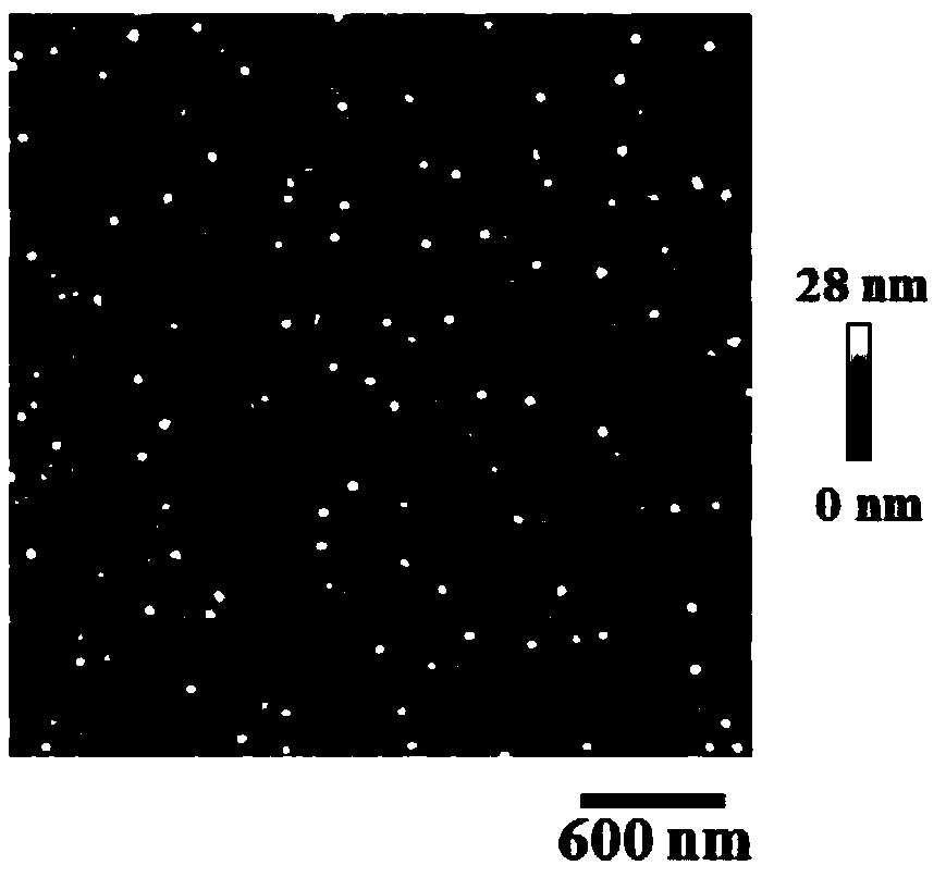
[0056] A preparation of polycarbazole derivative nanofibers, the steps of which are basically the same as in Example 1, and the similarities will not be repeated, except that the sum of the mass percentages of PCDTBT and PEO in the blending solution is 0.25wt %, PCDTBT and PEO blend films with a thickness of about 15nm were obtained.
[0057] like figure 2 As shown, the PCDTBT film on the silicon wafer has a network morphology composed of nanofibers and aggregates, and the width of the PCDTBT nanofibers is about 20nm.
Embodiment 3
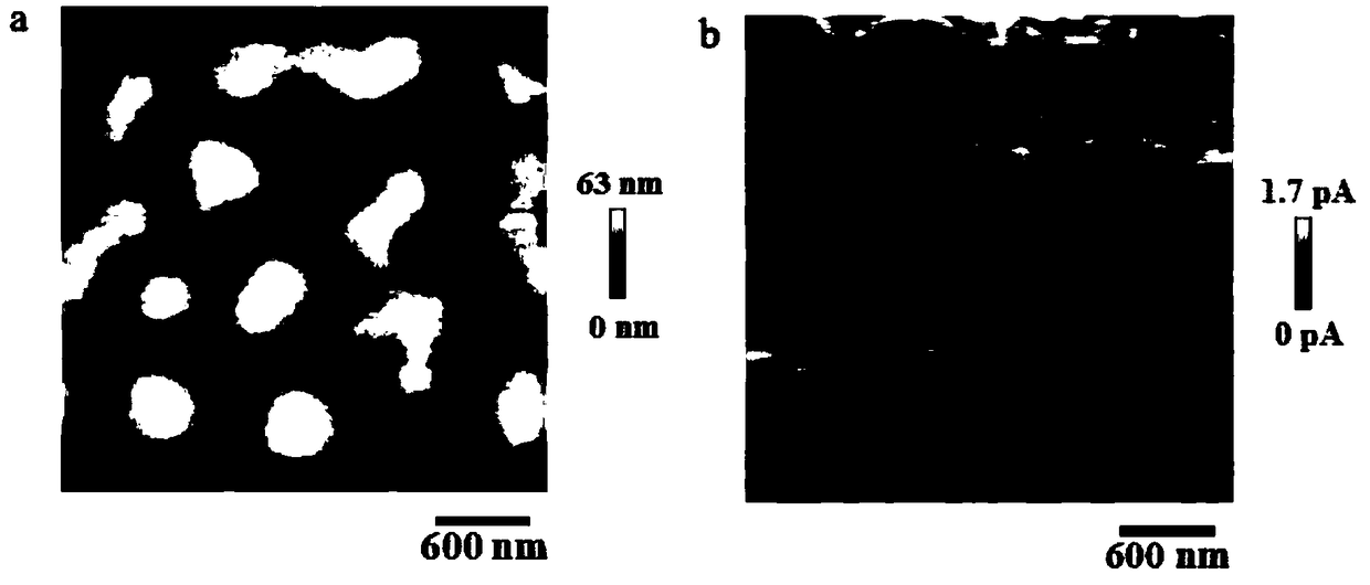
[0059] A preparation of polycarbazole derivative nanofibers, the steps of which are basically the same as in Example 1, and the similarities will not be repeated, except that the sum of the mass percentages of PCDTBT and PEO in the blending solution is 0.5wt %, PCDTBT and PEO blend films with a thickness of about 20nm were obtained.
[0060] like image 3 As shown, the PCDTBT film on the silicon wafer in figure a is a network morphology composed of nanofibers and aggregates, in which the width of PCDTBT nanofibers is about 20nm. The diagram of conductive atoms in b shows that PCDTBT nanofibers have obvious electrical signals and form a conductive network together with PCDTBT aggregates.
PUM
| Property | Measurement | Unit |
|---|---|---|
| width | aaaaa | aaaaa |
Abstract
Description
Claims
Application Information
 - R&D
- Intellectual Property
- Life Sciences
- Materials
- Tech Scout
- Unparalleled Data Quality
- Higher Quality Content
- 60% Fewer Hallucinations
Browse by: Latest US Patents, China's latest patents, Technical Efficacy Thesaurus, Application Domain, Technology Topic, Popular Technical Reports.
© 2025 PatSnap. All rights reserved.Legal|Privacy policy|Modern Slavery Act Transparency Statement|Sitemap|About US| Contact US: help@patsnap.com


