Film structure with electrical functionality and external contacting
A technology of thin film structure and electrical function, applied in cable insulation structure, conductive core parts, printed circuit parts, etc., can solve problems such as decreased conductivity and achieve the effect of less consumption
- Summary
- Abstract
- Description
- Claims
- Application Information
AI Technical Summary
Problems solved by technology
Method used
Image
Examples
Embodiment Construction
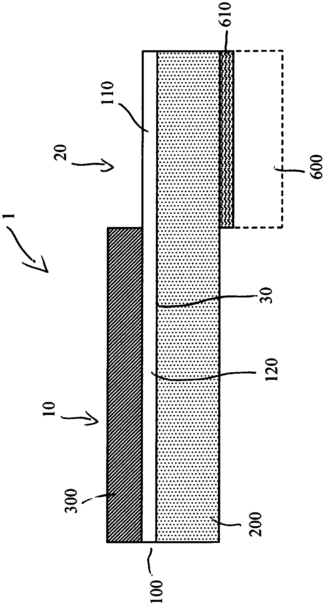
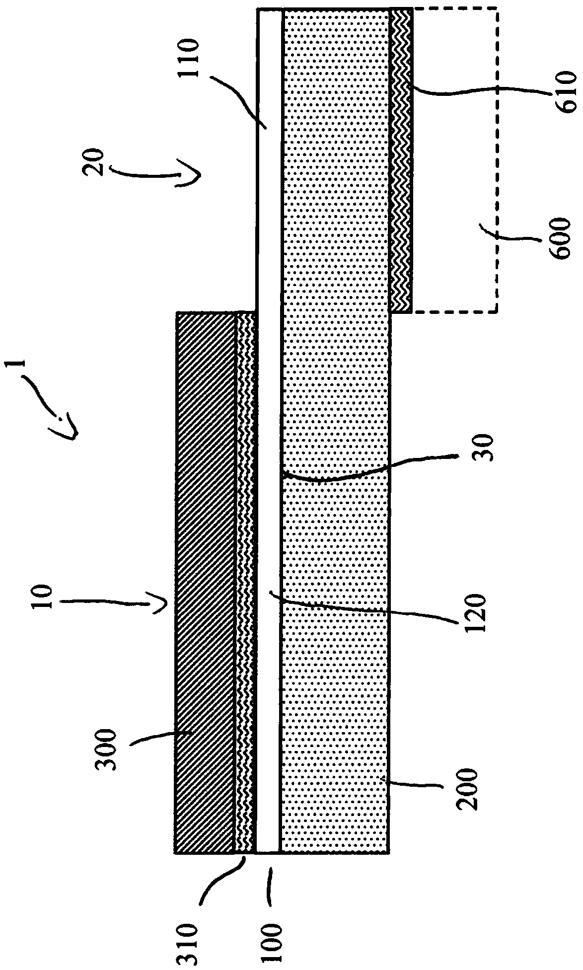
[0030] Figure 1A and 1B A lateral view of an embodiment of a thin-film structure 1 with electrical functions and external contacts is shown. The thin-film structure 1 has a region 10 with an electrical transmission path 30 and a contact region 20 for external contacting of the electrical transmission path 30 . At least one electrically conductive layer 100 comprising a material mixture of silver and carbon is contained in the contact region 20 .
[0031] In the thin film structure 1 Figure 1A and 1B In the embodiment shown in , the conductive layer 100 extends from the contact region 20 into the region 10 with the electrical transmission path 30 . Conductive layer 100 has a section 110 which is arranged in contact region 20 of film structure 1 . Furthermore, the electrically conductive layer 100 comprises a section 1230 which is connected to the section 110 which is arranged in the region 10 of the film structure having the electrical transmission path 30 . The electrica...
PUM
 Abstract
Description
Claims
Application Information
 - R&D
- Intellectual Property
- Life Sciences
- Materials
- Tech Scout
- Unparalleled Data Quality
- Higher Quality Content
- 60% Fewer Hallucinations
Browse by: Latest US Patents, China's latest patents, Technical Efficacy Thesaurus, Application Domain, Technology Topic, Popular Technical Reports.
© 2025 PatSnap. All rights reserved.Legal|Privacy policy|Modern Slavery Act Transparency Statement|Sitemap|About US| Contact US: help@patsnap.com


