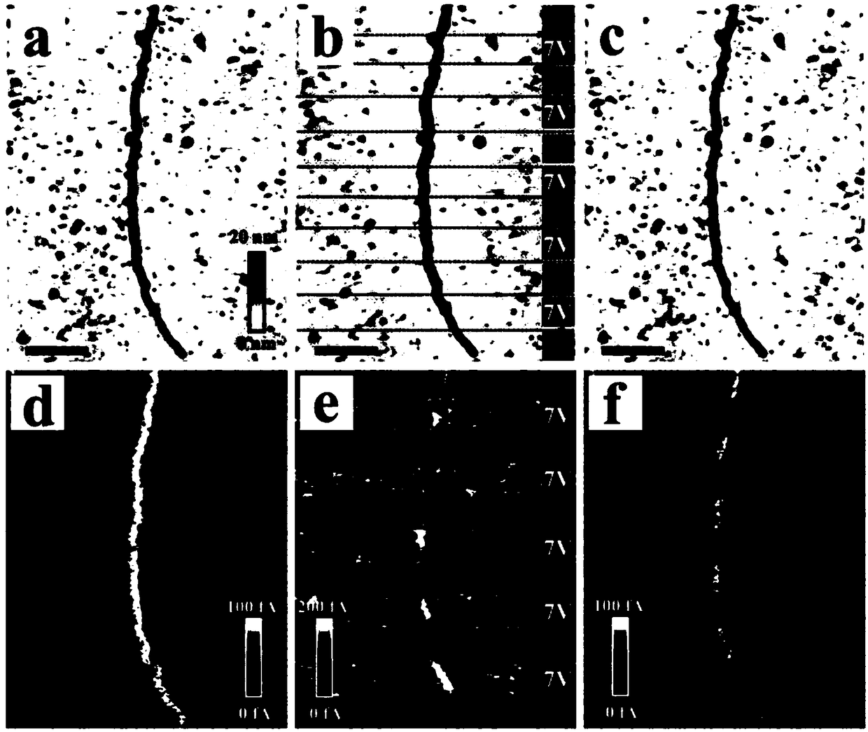
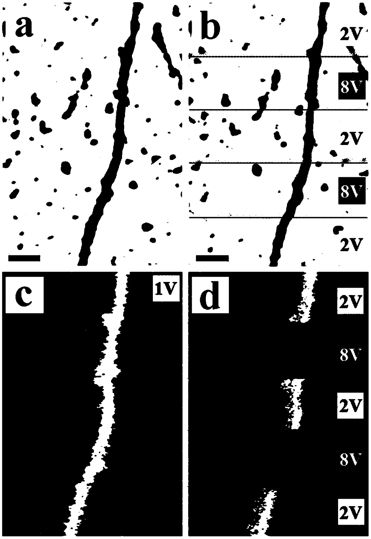
Method for constructing conjugated polymer nano-conductive pattern by scanning probe
A conjugated polymer, nano-conductive technology, applied in the direction of scanning probe technology, instruments, etc., can solve the problems of increasing the width of the scratch line, changing the surface shape of the material, affecting the processing accuracy, etc., to avoid energy waste, heat Less loss and less energy consumption
- Summary
- Abstract
- Description
- Claims
- Application Information
AI Technical Summary
Problems solved by technology
Method used
Image
Examples
Embodiment 1
[0056] In this embodiment to construct a conductive pattern, the conjugated polymer used is poly(3-hexylthiophene-2,5-diyl) (abbreviated as P3HT), and the number average molecular weight of the conjugated polymer is 5330 g / mol. The regularity of the conjugated polymer is greater than 90%.
[0057] A method for constructing a conjugated polymer nanoconductive pattern using a scanning probe, the method comprising the following steps:
[0058] (1) Take 1mg of conductive conjugated polymer P3HT, prepare a chlorobenzene solution of P3HT in a vial wrapped with aluminum foil, and the mass fraction of P3HT in the prepared P3HT chlorobenzene solution is 1.0wt%;
[0059] (2) Using a metal bath to heat the chlorobenzene solution of P3HT prepared in step (1), heating at 70°C for 6 hours to fully dissolve the conjugated polymer P3HT, and cooling to room temperature after the dissolution;
[0060] (3) Utilize a needle filter to filter the P3HT / chlorobenzene solution fully dissolved and coo...
Embodiment 2
[0066] In this embodiment, the conductive pattern is constructed, and the conjugated polymer used is P3HT. The number average molecular weight of the conjugated polymer is 17600 g / mol, and the regularity of the conjugated polymer is greater than 90%.
[0067] A method for constructing a conjugated polymer nanoconductive pattern using a scanning probe, the method comprising the following steps:
[0068](1) Take 1mg of conductive conjugated polymer P3HT, prepare a chlorobenzene solution of P3HT in a vial wrapped with aluminum foil, and the mass fraction of P3HT in the prepared P3HT chlorobenzene solution is 1.0wt%;
[0069] (2) Using a metal bath to heat the chlorobenzene solution of P3HT prepared in step (1), heating at 70°C for 6 hours to fully dissolve the conjugated polymer P3HT, and cooling to room temperature after the dissolution;
[0070] (3) Utilize a needle filter to filter the P3HT / chlorobenzene solution fully dissolved and cooled to room temperature in step (2), wher...
Embodiment 3
[0076] In this embodiment, the conductive pattern is constructed, and the conjugated polymer used is P3HT. The number average molecular weight of the conjugated polymer is 36600 g / mol, and the regularity of the conjugated polymer is greater than 90%.
[0077] A method for constructing a conjugated polymer nanoconductive pattern using a scanning probe, the method comprising the following steps:
[0078] (1) Take 2 mg of conductive conjugated polymer P3HT, prepare a chlorobenzene solution of P3HT in a vial wrapped with aluminum foil, and the mass fraction of P3HT in the prepared P3HT chlorobenzene solution is 2.0 wt %;
[0079] (2) Using a metal bath to heat the chlorobenzene solution of P3HT prepared in step (1), heating at 70°C for 6 hours to fully dissolve the conjugated polymer P3HT, and cooling to room temperature after the dissolution;
[0080] (3) Utilize a needle filter to filter the P3HT / chlorobenzene solution fully dissolved and cooled to room temperature in step (2), ...
PUM
| Property | Measurement | Unit |
|---|---|---|
| Thickness | aaaaa | aaaaa |
| Thickness | aaaaa | aaaaa |
| Thickness | aaaaa | aaaaa |
Abstract
Description
Claims
Application Information
 - R&D Engineer
- R&D Manager
- IP Professional
- Industry Leading Data Capabilities
- Powerful AI technology
- Patent DNA Extraction
Browse by: Latest US Patents, China's latest patents, Technical Efficacy Thesaurus, Application Domain, Technology Topic, Popular Technical Reports.
© 2024 PatSnap. All rights reserved.Legal|Privacy policy|Modern Slavery Act Transparency Statement|Sitemap|About US| Contact US: help@patsnap.com


