Double-layer phase change material, phase change memory cell and preparation method thereof
A phase-change material and double-layer technology, applied in the field of microelectronics, can solve the problems of low write operation current, high reliability, and slow programming speed of phase change speed, achieve improved power consumption and reliability, increase resistance ratio, The effect of fast phase change
- Summary
- Abstract
- Description
- Claims
- Application Information
AI Technical Summary
Problems solved by technology
Method used
Image
Examples
Embodiment 1
[0040] Using magnetron sputtering method, with Sb 2 Te 3 Preparation of induction layer Sb by co-sputtering of alloy target and Sb single substance target 2 Te phase-change material film, followed by magnetron sputtering on the induction layer Sb 2 Use Ge on Te 2 Sb 2 Te 5 Preparation of Ge by Alloy Target Sputtering 2 Sb 2 Te 5 phase change material thin film to prepare Ge 2 Sb 2 Te 5 / Sb 2 Te bilayer phase change material film layer.
[0041] The process parameters are: the background air pressure is 1×10 -5 Pa, Ar gas pressure is 0.2Pa during sputtering, sputtering power is Sb 2 Te 3 Alloy target 20W, Sb elemental target 10W, Ge 2 Sb 2 Te 5 The alloy target is 20W, and the substrate temperature is 25°C. By controlling the sputtering time, Ge 2 Sb 2 Te 5 / Sb2Te double-layer phase change material film thicknesses are 60nm / 20nm respectively.
[0042] In other embodiments, the atomic percentage of Sb in the Sb-Te phase change material in the induction layer...
Embodiment 2
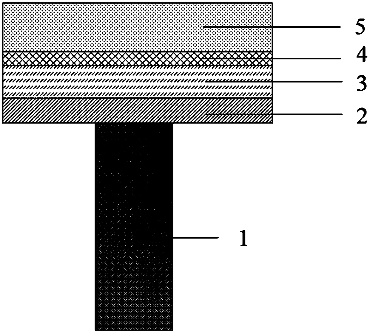
[0046] Such as figure 2 As shown, it is a schematic structural diagram of a phase-change memory cell of the present invention, the phase-change memory cell includes a lower electrode layer 1, an upper electrode layer 4, and a double layer between the lower electrode layer 1 and the upper electrode layer 4 Phase-change material layer 2,3; The double-layer phase-change material layer 2,3 adopts Ge-Sb-Te / Sb-Te double-layer phase-change material, and the chemical general formula of the described induction layer Sb-Te phase-change material is: Sb x Te 100-x , where x refers to the atomic percentage of the element, and satisfies 20<x<80.
[0047] Further, an extraction electrode 5 is also formed on the upper electrode layer 4 .
[0048] Contains Ge-Sb-Te / Sb x Te 100-x The preparation process of the phase-change memory device unit of the double-layer phase-change material is as follows:
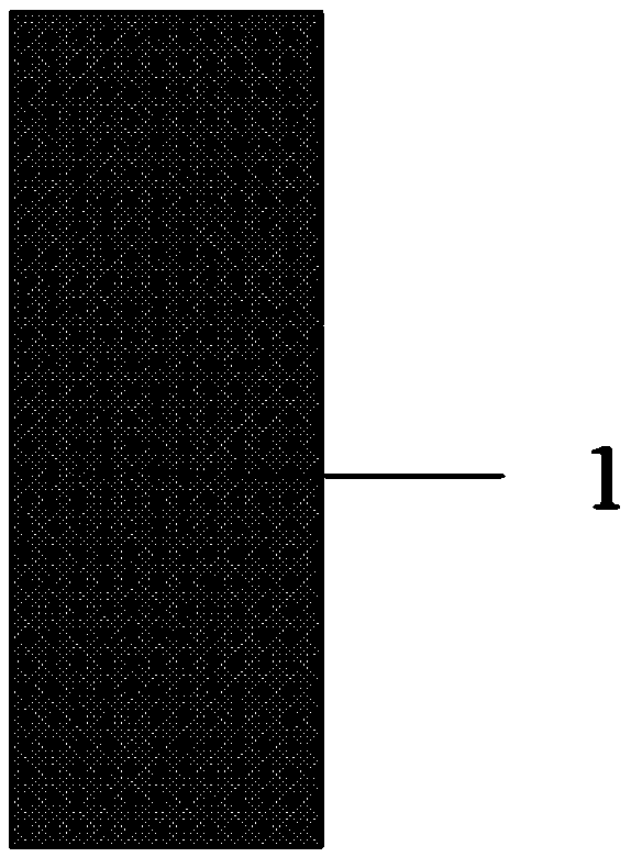
[0049] Step 1: See image 3 , by sputtering, evaporation, chemical vapor deposition, pla...
Embodiment 3
[0061] The electrical performance test of the phase change memory device unit in the above-mentioned embodiment is carried out as follows:
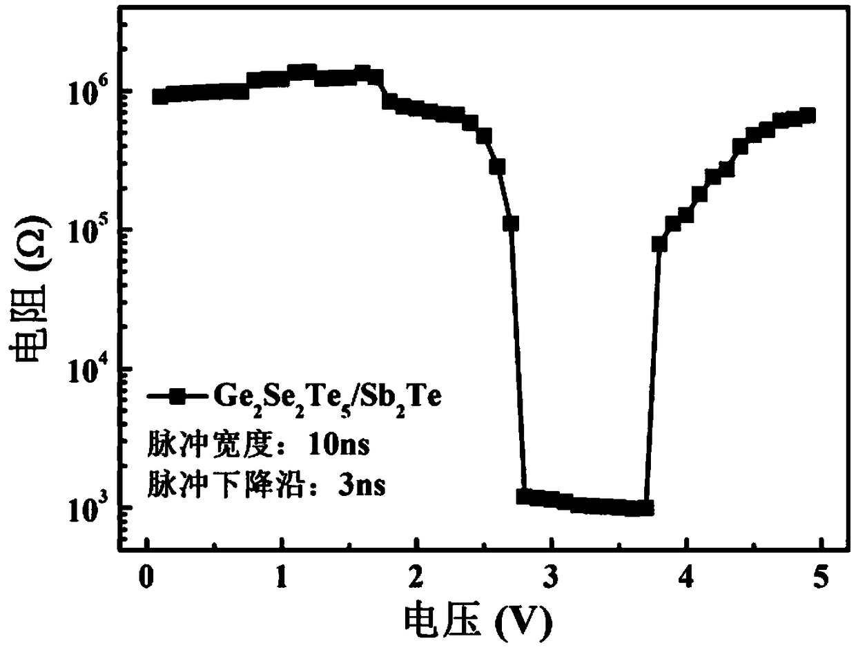
[0062] (1) The current-voltage (I-V) curve of the test device unit under the action of current excitation. For test results see Figure 7 . It can be seen that as the current increases, the voltage value continues to increase first, and at a certain point, the voltage suddenly drops to a very low level, and then continues to increase continuously. This point is the threshold point of the device unit, the voltage at this point is the threshold voltage, and the current is the threshold current. For Ge-based 2 Sb 2 Te 5 / Sb 2 The phase-change memory cell of Te has a measured threshold voltage of 0.87V and a threshold current of 9μA. At the threshold point, the phase change material transitions from an amorphous state to a crystalline state in a very short time, forming a low-resistance conduction path, resulting in a sudden drop in vo...
PUM
| Property | Measurement | Unit |
|---|---|---|
| thickness | aaaaa | aaaaa |
| diameter | aaaaa | aaaaa |
| height | aaaaa | aaaaa |
Abstract
Description
Claims
Application Information
 - R&D
- Intellectual Property
- Life Sciences
- Materials
- Tech Scout
- Unparalleled Data Quality
- Higher Quality Content
- 60% Fewer Hallucinations
Browse by: Latest US Patents, China's latest patents, Technical Efficacy Thesaurus, Application Domain, Technology Topic, Popular Technical Reports.
© 2025 PatSnap. All rights reserved.Legal|Privacy policy|Modern Slavery Act Transparency Statement|Sitemap|About US| Contact US: help@patsnap.com


