
Built-in longitudinal heat dissipation ceramic block print circuit board and circuit assembly provided with that circuit board

A technology for printed circuit boards and ceramic blocks, applied in the directions of printed circuit components, printed circuits, printed circuits, etc., can solve the problems of expensive machines, inability to reduce the width and spacing of wires, and process limitations, so as to reduce the area of ​​ceramic materials, Good thermal conductivity, increase the effect of elasticity

Active Publication Date: 2018-12-11
ICP TECH +1
View PDF6 Cites 4 Cited by
  • Summary
  • Abstract
  • Description
  • Claims
  • Application Information

AI Technical Summary

Problems solved by technology

[0009] However, in practice, if you want to use a printed circuit board made of ceramic material substrates, although the wire diameter of the circuit can be as thin as 30 microns (μm), due to the high temperature firing usually used, a small amount of Uneven expansion and warping, so the precision of the substrate is not as good as that of the printed circuit board and is not suitable for the manufacture of multi-layer boards; on the other hand, the metal atoms that make up the circuit are easy to diffuse freely during the high-temperature process, so that the distance between the wires must be maintained at 80 microns (μm )about
Therefore, the use of ceramic material substrates to make printed circuit boards not only increases the cost, but also causes the width and spacing of the wires to be reduced, as well as the accuracy of the position of the wire lines, making it impossible to miniaturize the size of electronic devices using the entire ceramic material substrate.
[0010] Therefore, for electronic components with high heat generation, the electronic components are often placed on a small piece of ceramics first, and then placed on a resin printed circuit board to form a stacked structure, which not only increases the volume of the printed circuit board , and because the ceramic block and the heat conduction element need to pass through the material with poor thermal conductivity, it will reduce the original heat dissipation efficiency
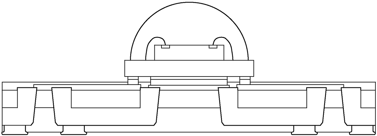
[0011] For example, someone in the industry proposed to use semiconductor manufacturing process to deposit heat dissipation material on the etched dielectric substrate to make such a figure 1 The composite heat-dissipating substrate is shown; however, because the semiconductor manufacturing process is quite expensive, the cost of this manufacturing method is high, especially considering the cost sharing of the photomask in the manufacturing process, so it is not suitable for a small number of various products. The manufacturing process is quite limited, and it is not widely used by general substrate factories

Method used


Image

  • Built-in longitudinal heat dissipation ceramic block print circuit board and circuit assembly provided with that circuit board
  • Built-in longitudinal heat dissipation ceramic block print circuit board and circuit assembly provided with that circuit board
  • Built-in longitudinal heat dissipation ceramic block print circuit board and circuit assembly provided with that circuit board

Examples


Embodiment Construction

[0038] The aforementioned and other technical content, features and effects of the present invention will be clearly presented in the following detailed description of the preferred embodiments in conjunction with the accompanying drawings; in addition, in each embodiment, the same elements will be similar The label indicates.

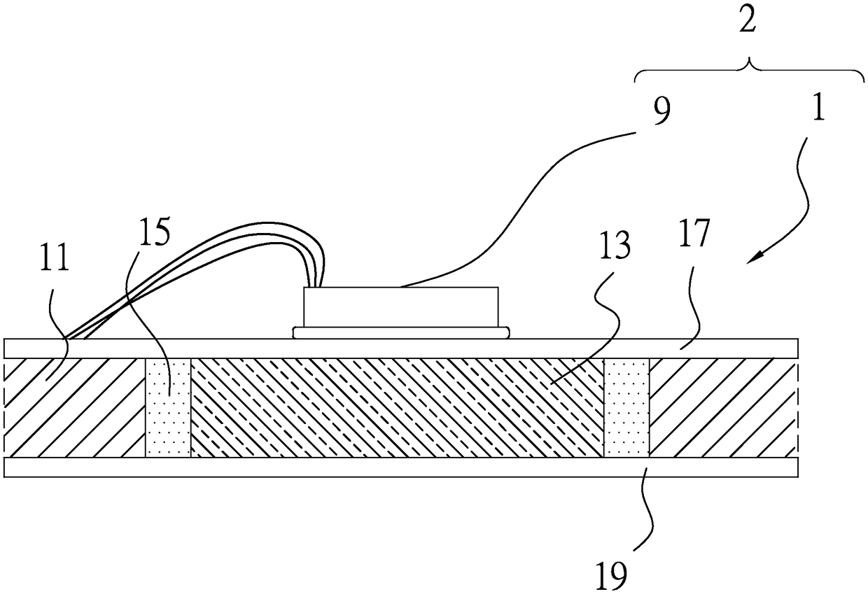
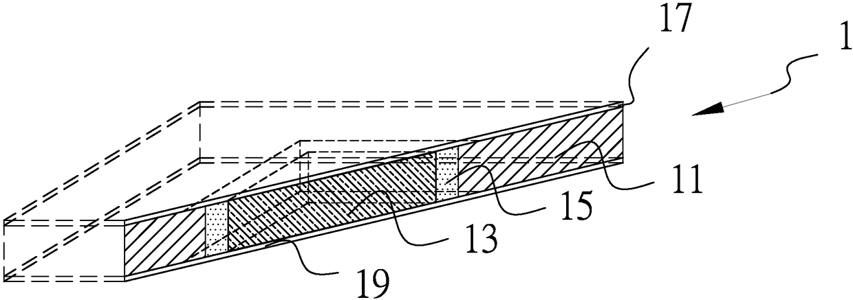
[0039] A first preferred embodiment of a printed circuit board with a built-in vertical heat dissipation ceramic block of the present invention and a circuit assembly with the printed circuit board, such as Figure 2 to Figure 5 As shown, it is based on the multi-layer dielectric material layer 11 of FR-4 with a length and a width of 10 cm. In the dielectric material layer 11, for example, a through hole 115 with a length and a width of 2 cm is pre-cut in the dielectric material layer 11. Then the corresponding aluminum oxide (Al 2 o 3 ) The heat-dissipating ceramic block 13 made of a square column is embedded in the through hole 115 . However, as t...


PUM


Abstract

A longitudinal heat dissipation ceramic block built-in print circuit board and a circuit assembly provided with that circuit board, wherein the circuit assembly comprise: a printed circuit board built-in longitudinal heat dissipation ceramic block and a plurality of circuit elements; the printed circuit board further comprises a dielectric material lay and forms at least one through hole; At leastone correspond heat dissipation ceramic block embedded in that through hole; At least one fixing portion for fixing the heat dissipation ceramic block in the through hole; A metal circuit lay disposed on that upper surface of the dielectric material lay and the heat dissipation ceramic block and a high heat conduction layer disposed on the lower surface of the ceramic block. The invention can adjust the position and size of the heat dissipation ceramic block according to the need, so as to achieve the purpose of adapting to the complex circuit design, exerting good heat conduction effect andcontrolling the heat energy conduction path, and reducing the manufacturing cost.

Description

technical field [0001] A printed circuit board, especially a printed circuit board with a built-in vertical heat dissipation ceramic block and a circuit assembly with the circuit board. Background technique [0002] The printed circuit board (Printed Circuit Board, PCB) is based on the copper foil substrate as the main key basic material for the installation of electronic components. The copper foil substrate generally uses dielectric materials as the insulating layer, and the wires formed by copper foil are used as the The conductive material layer is formed by arranging the conductive material layer on the dielectric insulating layer. Among them, the dielectric materials are mostly paper, bakelite, glass fiber board, rubber and other types of polymers and other insulating materials impregnated with resin. For the convenience of subsequent description, the present invention refers to the insulating layer of the copper foil substrate as a dielectric material layer. [0003...

Claims


Application Information

Patent Timeline
Patent Type & Authority Applications(China)
IPC IPC(8): H05K1/02H05K1/03
CPCH05K1/0203H05K1/0306H05K2201/09063
Inventor 余河洁廖政龙林俊佑黄安正
Owner ICP TECH
Learn More