Preparation method of a microfluidic array controller
An array controller and microfluidic technology, applied in chemical instruments and methods, laboratory equipment, laboratory containers, etc., can solve problems such as difficult to realize large-scale fluid array control, reduce the number of leads and reduce the control voltage , the effect of meeting the needs of use
- Summary
- Abstract
- Description
- Claims
- Application Information
AI Technical Summary
Problems solved by technology
Method used
Image
Examples
Embodiment 1
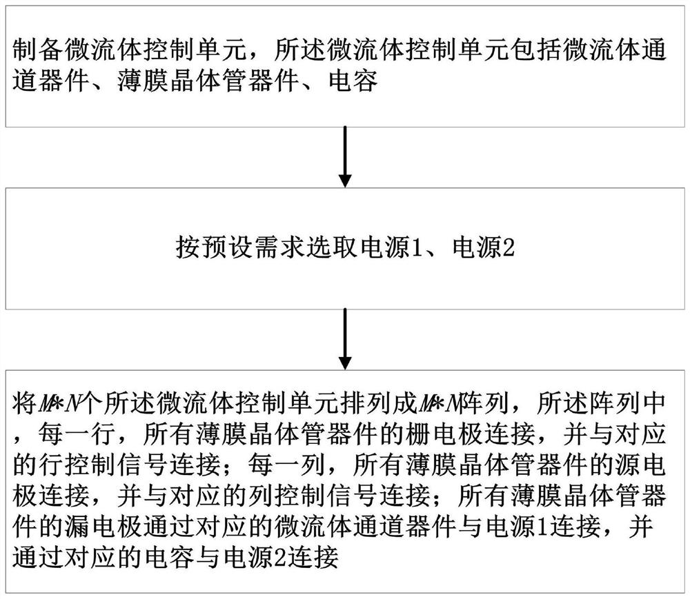
[0071] like figure 2 As shown, a specific embodiment of the present invention discloses a method for preparing a microfluidic array controller, comprising the following steps:
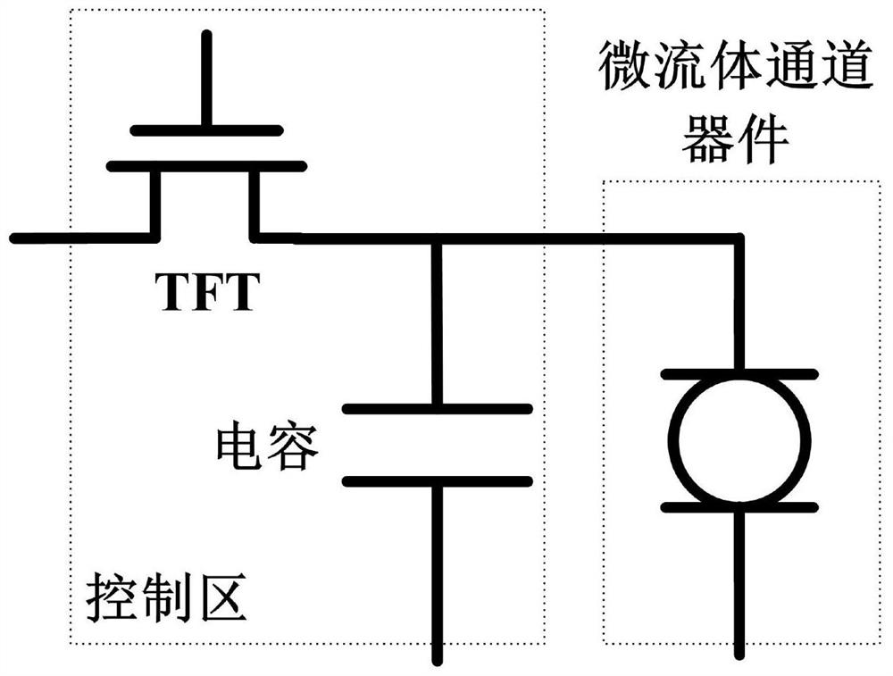
[0072] S1. Prepare a microfluidic control unit, the microfluidic control unit includes a microfluidic channel device, a thin film transistor device, and a capacitor.
[0073] S2. Select power supply 1 and power supply 2 according to preset requirements.
[0074] S3. Arranging M×N microfluidic control units into an M×N array, in the array, in each row, the gate electrodes of all thin film transistor devices are connected, and are connected to the corresponding row control signals; in each column, all The source electrodes of the thin film transistor devices are connected to the corresponding column control signals; the drain electrodes of all the thin film transistor devices are connected to the power source 1 through the corresponding microfluidic channel devices, and connected to the power source 2 ...
Embodiment 2
[0081] like Figure 5 As shown, optimization is carried out on the basis of the foregoing examples, and the steps of preparing the microfluidic control unit include:
[0082] S11. Prepare the control layer of the microfluidic control unit on the silicon wafer or the first glass substrate, and the control layer includes thin film transistor devices and capacitors.
[0083] S12. Prepare a passivation layer on the control layer, and make through holes at preset positions on the passivation layer. The process of preparing the passivation layer is chemical vapor deposition or physical vapor deposition, and the material used is at least one of silicon oxide, hafnium oxide, aluminum oxide, titanium oxide, silicon nitride, and parylene, with a thickness of 100nm to 2μm . The process of making via holes on the passivation layer is photolithography and etching process. The preset position of the through hole is above the drain electrode of the thin film transistor.
[0084] S13. Pre...
PUM
 Abstract
Description
Claims
Application Information
 - R&D
- Intellectual Property
- Life Sciences
- Materials
- Tech Scout
- Unparalleled Data Quality
- Higher Quality Content
- 60% Fewer Hallucinations
Browse by: Latest US Patents, China's latest patents, Technical Efficacy Thesaurus, Application Domain, Technology Topic, Popular Technical Reports.
© 2025 PatSnap. All rights reserved.Legal|Privacy policy|Modern Slavery Act Transparency Statement|Sitemap|About US| Contact US: help@patsnap.com


