A preparation method based on helium-containing w-based nanocrystalline thin film material
A technology of thin film materials and nanocrystals, which is applied in metal material coating process, vacuum evaporation coating, coating, etc., can solve the problems of radio frequency magnetron sputtering that have not been seen, and meet the needs of large-scale sample research. The effect of simple and easy-to-operate preparation process
- Summary
- Abstract
- Description
- Claims
- Application Information
AI Technical Summary
Problems solved by technology
Method used
Image
Examples
Embodiment 1
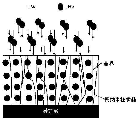
[0027] This embodiment provides a method for preparing a helium-containing W-based nanocrystalline thin film material, such as figure 1 As shown, including the following steps:
[0028] Step 1: Perform surface treatment on the W target (the thickness of the W target is 2mm), remove the surface metal oxide and impurities, and obtain the metal W target to be sputtered;
[0029] Step 2: The single crystal Si substrate is ultrasonically cleaned with a mixed solution of alcohol and acetone, and finally rinsed with deionized water and dried;
[0030] Step 3: Mount the W target of step 1 on the permanent magnet target of magnetron sputtering, put the substrate of step 2 on the substrate in the magnetron sputtering apparatus, vacuum to 8×10⁻⁵Pa, and pass in He / Ar mixed atmosphere was sputtered and deposited for 5h, where the total pressure of He / Ar mixed gas was 2Pa, the He / Ar pressure ratio was 5; the deposition temperature of single crystal Si substrate was normal temperature -600℃, and th...
Embodiment 2
[0036] This embodiment provides a method for preparing helium-containing W-based nanocrystalline thin film material. Compared with Example 1, the process parameters of step 2 and step 3 are the same. The difference is that the W-based target material used in step 1 is W Alloy target (oxide dispersion W or carbide dispersion W).
[0037] The helium-containing W-based nanocrystalline thin film material obtained by the method described in this embodiment was tested according to the method described in Example 1, and the results showed that:
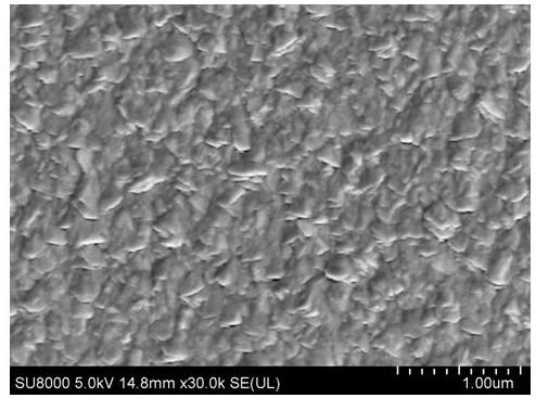
[0038] The grain size of the helium-containing W-based nanocrystalline thin film material is about 100nm, which is in line with the size range of nanocrystalline materials;
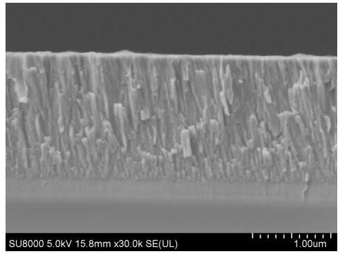
[0039] The crystal structure of the helium-containing W nanocrystalline thin film material is a typical nano columnar crystal, and the thickness of the thin film is in the range of 10nm-100μm.
[0040] The distribution of helium bubbles in the helium-containing W nanocrystallin...
Embodiment 3
[0042] This embodiment provides a method for preparing a helium-containing W-based nanocrystalline thin film material. Compared with embodiment 1, the process parameters of step 1 and step 3 are the same, but the difference is that the substrate in step 2 is a ceramic substrate .
[0043] The helium-containing W-based nanocrystalline thin film material obtained by the method described in this embodiment was tested according to the method described in Example 1, and the results showed that:
[0044] The grain size of the helium-containing W-based nanocrystalline thin film material is about 100nm, which is in line with the size range of nanocrystalline materials;
[0045] The crystal structure of the helium-containing W nanocrystalline thin film material is a typical nano columnar crystal, and the thickness of the thin film is in the range of 10nm-100μm.
[0046] The distribution of helium bubbles in the helium-containing W nanocrystalline thin film material is uniform, and the average ...
PUM
| Property | Measurement | Unit |
|---|---|---|
| thickness | aaaaa | aaaaa |
| thickness | aaaaa | aaaaa |
| particle size | aaaaa | aaaaa |
Abstract
Description
Claims
Application Information
 - R&D
- Intellectual Property
- Life Sciences
- Materials
- Tech Scout
- Unparalleled Data Quality
- Higher Quality Content
- 60% Fewer Hallucinations
Browse by: Latest US Patents, China's latest patents, Technical Efficacy Thesaurus, Application Domain, Technology Topic, Popular Technical Reports.
© 2025 PatSnap. All rights reserved.Legal|Privacy policy|Modern Slavery Act Transparency Statement|Sitemap|About US| Contact US: help@patsnap.com


