
Outline structure of a contact hole

A contact hole and shape technology, which is applied in the manufacture of electrical components, circuits, semiconductors/solid-state devices, etc., can solve problems such as difficult copper deposition, voids, and unstable electrical properties, so as to improve output and quality, avoid voids, The effect of improving electrical performance

Active Publication Date: 2021-01-12
WUHAN XINXIN SEMICON MFG CO LTD
View PDF5 Cites 0 Cited by
  • Summary
  • Abstract
  • Description
  • Claims
  • Application Information

AI Technical Summary

Problems solved by technology

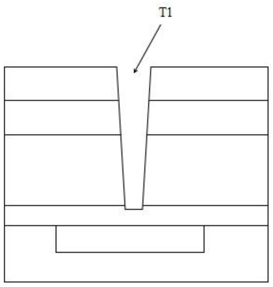
[0003] Currently, if figure 1 As shown, in the traditional process, the contact hole T1 is designed as a linear shape. When depositing tungsten on the contact hole T1 with a small size, it is difficult to form a barrier layer and a seed layer, which makes the electrical performance unstable. It is very difficult to deposit copper, and it is also difficult to meet the requirements of copper deposition. It is easy to form voids, which will affect the yield and quality of wafers.

Method used


Image

  • Outline structure of a contact hole
  • Outline structure of a contact hole

Examples


Embodiment Construction

[0034] The following will clearly and completely describe the technical solutions in the embodiments of the present invention with reference to the accompanying drawings in the embodiments of the present invention. Obviously, the described embodiments are only some, not all, embodiments of the present invention. Based on the embodiments of the present invention, all other embodiments obtained by persons of ordinary skill in the art without creative efforts fall within the protection scope of the present invention.

[0035] It should be noted that, in the case of no conflict, the embodiments of the present invention and the features in the embodiments can be combined with each other.

[0036] The present invention will be further described below in conjunction with the accompanying drawings and specific embodiments, but not as a limitation of the present invention.

[0037] The present invention includes a shape structure of a contact hole, which includes:

[0038] A semicondu...


PUM

PropertyMeasurementUnit
sizeaaaaaaaaaa
sizeaaaaaaaaaa
sizeaaaaaaaaaa

Abstract

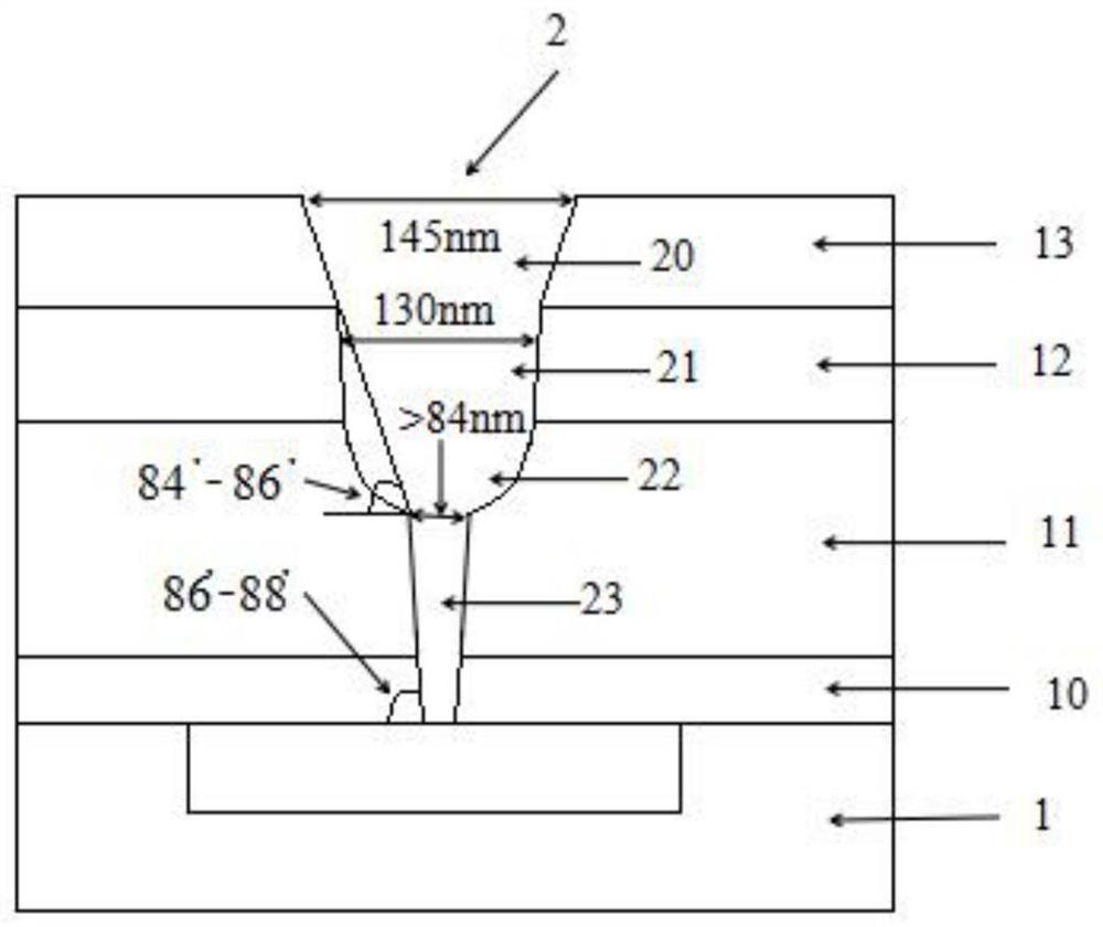
The invention discloses an outline structure of a contact hole, wherein a semiconductor structure is provided, the semiconductor structure includes a substrate, and a first nitride layer, a first oxide layer, a second nitride layer and a second oxide layer are sequentially deposited on the substrate ; Form a contact hole on the semiconductor structure, including a first section, a second section, a third section and a fourth section; the first section is located at the upper port and the lower part of the second oxide layer from top to bottom along the slope Between the ports; the second section is located between the upper port and the lower port of the second nitride layer from top to bottom along the slope, and the upper end opening of the second section is the same as the lower end opening of the first section; the third section Located between the upper part and the middle part of the first oxide layer, the third section is an arc-shaped structure, and the arc-shaped structure protrudes to both sides of the third section; the fourth section is located between the middle part of the first oxide layer and the first nitriding layer. Between the lower ports of the layer. The beneficial effect is that the shape structure of the contact hole is changed, and the depth-to-width ratio of the contact hole is indirectly reduced, thereby avoiding the occurrence of voids.

Description

technical field [0001] The invention relates to the technical field of semiconductor technology, in particular to an outline structure of a contact hole. Background technique [0002] With the development of the semiconductor process, the technical requirements of the semiconductor are becoming more and more stringent, and the size of the contact hole is continuously reduced, which poses more and more challenges to the deposition of the contact hole. [0003] Currently, if figure 1 As shown, in the traditional process, the contact hole T1 is designed as a linear shape. When depositing tungsten on the contact hole T1 with a small size, it is difficult to form a barrier layer and a seed layer, which makes the electrical performance unstable. It is very difficult to deposit copper, and it is also difficult to meet the requirements of copper deposition, and it is easy to form voids, which in turn affects the yield and quality of wafers. Contents of the invention [0004] In ...

Claims


Application Information

Patent Timeline
Patent Type & Authority Patents(China)
IPC IPC(8): H01L21/768
CPCH01L21/76802H01L21/76897
Inventor 宋保英
Owner WUHAN XINXIN SEMICON MFG CO LTD
Learn More