Non-refrigeration terahertz detector with adjustable working frequency
A terahertz detector and operating frequency technology, which is applied to thermoelectric devices with thermal changes in dielectric constant, etc., can solve the problems of slow response speed and long time of the device, and achieve the effect of simple structure, good thermal insulation performance and good application prospect.
- Summary
- Abstract
- Description
- Claims
- Application Information
AI Technical Summary
Problems solved by technology
Method used
Image
Examples
Embodiment 1
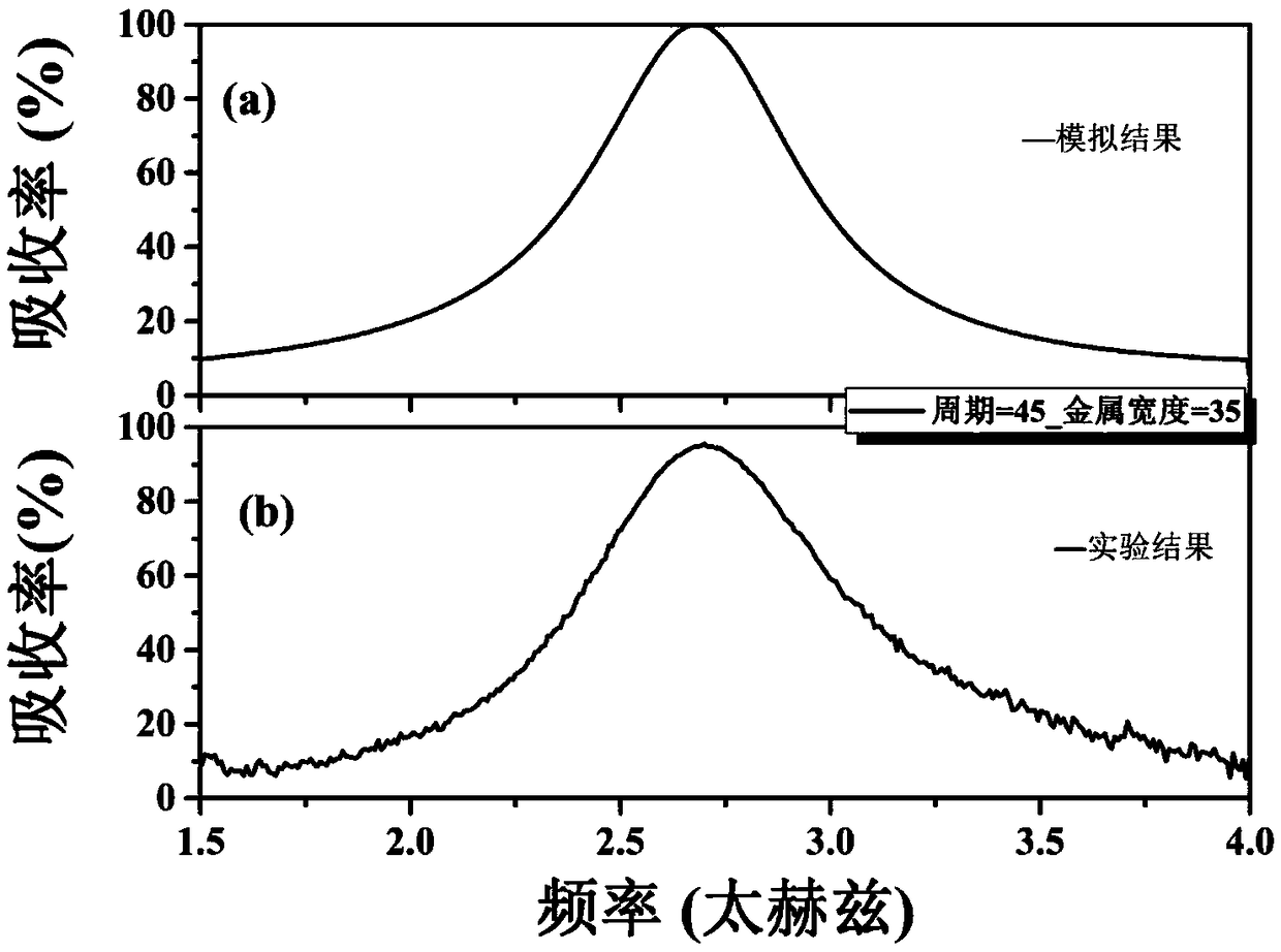
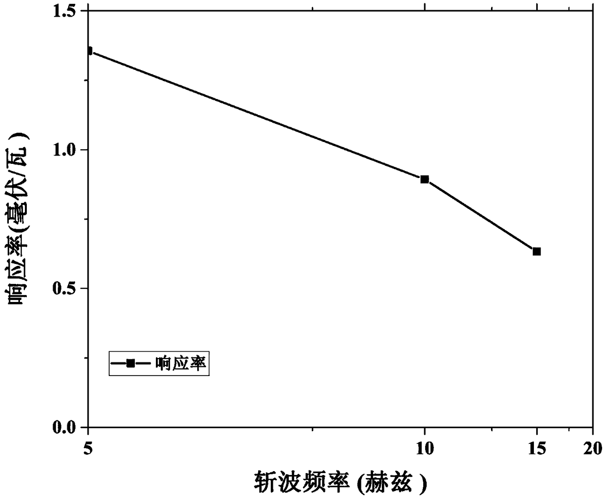
[0018] An uncooled terahertz detector with adjustable working frequency. In this embodiment, Si is selected as the substrate. First, the substrate is cleaned, and then a layer of polyimide film is spin-coated on its surface, and then a gold film is plated on the polyimide film by electron beam evaporation, and then spin-coated to prepare For the dielectric cavity layer, UV lithography is used to transfer the top layer pattern, and then the top layer metal is plated, followed by wet stripping, and finally optical and electrical tests are performed. The specific implementation steps are as follows:
[0019] 1. Substrate cleaning. Put the Si wafer in alcohol for 10 minutes and ultrasonically remove the oil on the surface of the substrate. After ultrasonic cleaning, quickly take it out and dry it with nitrogen.
[0020] 2. Preparation of polyimide film. A layer of polyimide film was spin-coated on the Si wafer, followed by annealing at 80° C., 120° C., 150° C., 180° C., and 250...
Embodiment 2
[0028] An uncooled terahertz detector with adjustable working frequency. In this embodiment, Si is selected as the substrate. First, the substrate is cleaned, and then a layer of polyimide film is spin-coated on its surface, and then a gold film is plated on the polyimide film by electron beam evaporation, and then spin-coated to prepare For the dielectric cavity layer, UV lithography is used to transfer the top layer pattern, and then the top layer metal is plated, followed by wet stripping, and finally optical and electrical tests are performed. The specific implementation steps are as follows:
[0029] 1. Substrate cleaning. Put the Si wafer in alcohol for 10 minutes and ultrasonically remove the oil on the surface of the substrate. After ultrasonic cleaning, quickly take it out and dry it with nitrogen.
[0030] 2. Preparation of polyimide film. A layer of polyimide film was spin-coated on the Si wafer, followed by annealing at 80°C, 120°C, 150°C, 180°C, and 250°C for o...
Embodiment 3
[0038] An uncooled terahertz detector with adjustable working frequency. In this embodiment, Si is selected as the substrate. First, the substrate is cleaned, and then a layer of polyimide film is spin-coated on its surface, and then a gold film is plated on the polyimide film by electron beam evaporation, and then spin-coated to prepare For the dielectric cavity layer, UV lithography is used to transfer the top layer pattern, and then the top layer metal is plated, followed by wet stripping, and finally optical and electrical tests are performed. The specific implementation steps are as follows:
[0039] 1. Substrate cleaning. Put the Si wafer in alcohol for 10 minutes and ultrasonically remove the oil on the surface of the substrate. After ultrasonic cleaning, quickly take it out and dry it with nitrogen.
[0040] 2. Preparation of polyimide film. A layer of polyimide film was spin-coated on the Si wafer, followed by annealing at 80°C, 120°C, 150°C, 180°C, and 250°C for o...
PUM
 Abstract
Description
Claims
Application Information
 - R&D
- Intellectual Property
- Life Sciences
- Materials
- Tech Scout
- Unparalleled Data Quality
- Higher Quality Content
- 60% Fewer Hallucinations
Browse by: Latest US Patents, China's latest patents, Technical Efficacy Thesaurus, Application Domain, Technology Topic, Popular Technical Reports.
© 2025 PatSnap. All rights reserved.Legal|Privacy policy|Modern Slavery Act Transparency Statement|Sitemap|About US| Contact US: help@patsnap.com


