A high-performance optoelectronic device based on carbon nanotube/graphene Schottky junction
A carbon nanotube, optoelectronic device technology, applied in electrical components, photovoltaic power generation, semiconductor devices, etc., can solve the problems of limiting the detectability of devices, large dark current of devices, etc., to improve optoelectronic performance, reduce dark current, and improve light absorption effect
- Summary
- Abstract
- Description
- Claims
- Application Information
AI Technical Summary
Problems solved by technology
Method used
Image

Examples
Embodiment 1
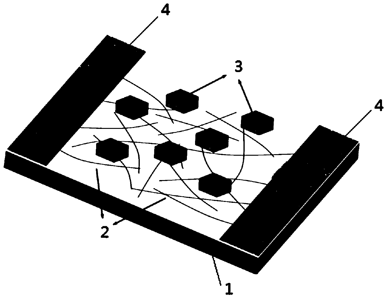
[0023] This embodiment provides a high-performance photoconductive detector based on carbon nanotube / graphene Schottky junction, and its structural diagram is as follows figure 1 shown. The photoconductive device includes an insulating substrate 1, a carbon nanotube network 2, an island graphene 3, and a patterned electrode 4, and its construction method is as follows:
[0024] (1) Si / SiO 2 (300nm) substrate as an insulating base, in Si / SiO 2 (300nm) island-shaped CVD graphene is transferred on the substrate by wet transfer method;
[0025] (2) A patterned Au electrode pair is deposited using a traditional micromachining process, and the island-shaped graphene outside the channel is removed by oxygen plasma etching;
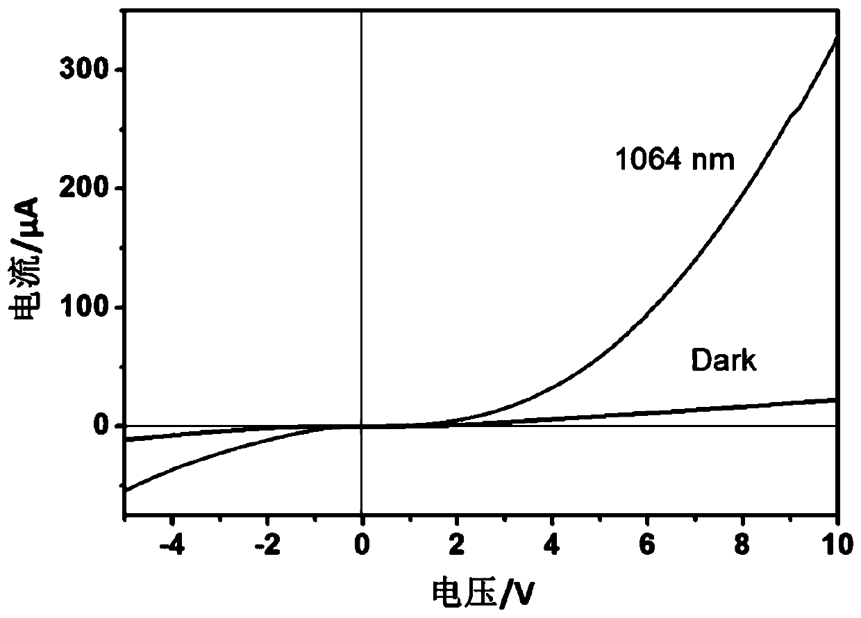
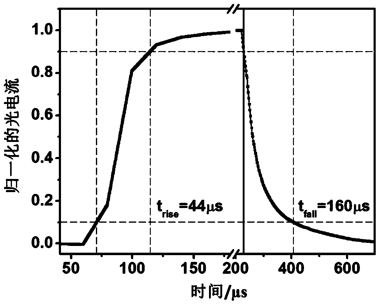
[0026] (3) The semiconducting SWCNTs network (10nm) was deposited between the Au electrode pair by drop-coating method. Promptly obtain high-performance photoconductive detector, it is irradiated by 1064nm laser (30mW / cm 2 ) under the condition of photoelect...
Embodiment 2
[0028] This embodiment provides a high-performance field-effect transistor photodetector based on carbon nanotube / graphene Schottky junction, and its structural diagram is as follows Figure 4 shown. The photoconductive device is composed of a gate 8, a gate dielectric layer 7, a carbon nanotube network 2, an island graphene 3, a source 5, and a drain 6, and its construction method is as follows:
[0029] (1) Use highly doped Si as the gate, and thermally oxidize and grow SiO on its surface 2 (300nm) is the gate dielectric layer.
[0030] (2)Si / SiO 2 The island-shaped CVD graphene is transferred on the substrate by wet transfer method;
[0031] (3) A patterned Au electrode pair is deposited as a source-drain electrode using a traditional micromachining process, and the island-shaped graphene outside the channel is removed by oxygen plasma etching;
[0032] (4) The semiconducting SWCNTs network (15nm) was deposited between the source and drain electrodes by transfer method....
Embodiment 3
[0034] This embodiment provides a high-performance photoconductive detector based on carbon nanotube / graphene Schottky junction. The photoconductive device includes an insulating substrate, a semiconducting SWCNTs network, patterned graphene, and patterned electrodes. Its construction method is as follows:
[0035] (1) Transfer CVD continuous graphene to Si / SiO by wet transfer method 2 (300nm) on the substrate;
[0036] (2) Patterned graphene was obtained by traditional photolithography process and oxygen plasma treatment process.
[0037] (3) A patterned Au electrode pair is deposited using a traditional micromachining process, and the patterned graphene outside the channel is removed by oxygen plasma etching;
[0038] (4) The semiconducting SWCNTs network (1nm) was deposited on the patterned graphene surface by spin-coating method and connected to the Au electrode. That is, a high-performance photoconductive detector is obtained.
PUM
| Property | Measurement | Unit |
|---|---|---|
| thickness | aaaaa | aaaaa |
| thickness | aaaaa | aaaaa |
| thickness | aaaaa | aaaaa |
Abstract
Description
Claims
Application Information
 - R&D
- Intellectual Property
- Life Sciences
- Materials
- Tech Scout
- Unparalleled Data Quality
- Higher Quality Content
- 60% Fewer Hallucinations
Browse by: Latest US Patents, China's latest patents, Technical Efficacy Thesaurus, Application Domain, Technology Topic, Popular Technical Reports.
© 2025 PatSnap. All rights reserved.Legal|Privacy policy|Modern Slavery Act Transparency Statement|Sitemap|About US| Contact US: help@patsnap.com