A silicon carbide mosfet drive circuit

A drive circuit, silicon carbide technology, applied in electronic switches, electrical components, high-efficiency power electronic conversion, etc., can solve the problems of low upper limit of gate turn-on voltage, device gate breakdown damage, low gate turn-on voltage, etc., to achieve Effects of reducing crosstalk, increasing switching speed, and reducing switching loss

Active Publication Date: 2020-02-14
NORTHWESTERN POLYTECHNICAL UNIV
View PDF4 Cites 0 Cited by
  • Summary
  • Abstract
  • Description
  • Claims
  • Application Information

AI Technical Summary

Problems solved by technology

Compared with silicon MOSFETs, silicon carbide MOSFETs have the advantages of small on-resistance, fast switching speed, and high blocking voltage, but the gate turn-on voltage of silicon carbide MOSFETs is low, and they are more susceptible to interference under high-voltage and high-frequency switching states False conduction occurs, and the upper limit of gate turn-on voltage is low, and gate voltage spikes during operation are more likely to cause breakdown and damage to the gate of the device. These characteristics limit the application of silicon carbide, and silicon carbide MOSFETs cannot be simply used in practical applications. To directly replace silicon MOSFETs, corresponding drive circuits must be designed to ensure safe and reliable operation of silicon carbide MOSFETs and give full play to the performance advantages of silicon carbide MOSFETs

Method used


Image

  • A silicon carbide mosfet drive circuit
  • A silicon carbide mosfet drive circuit

Examples


Embodiment Construction

[0016] The present invention will be further described below in conjunction with the accompanying drawings and embodiments.

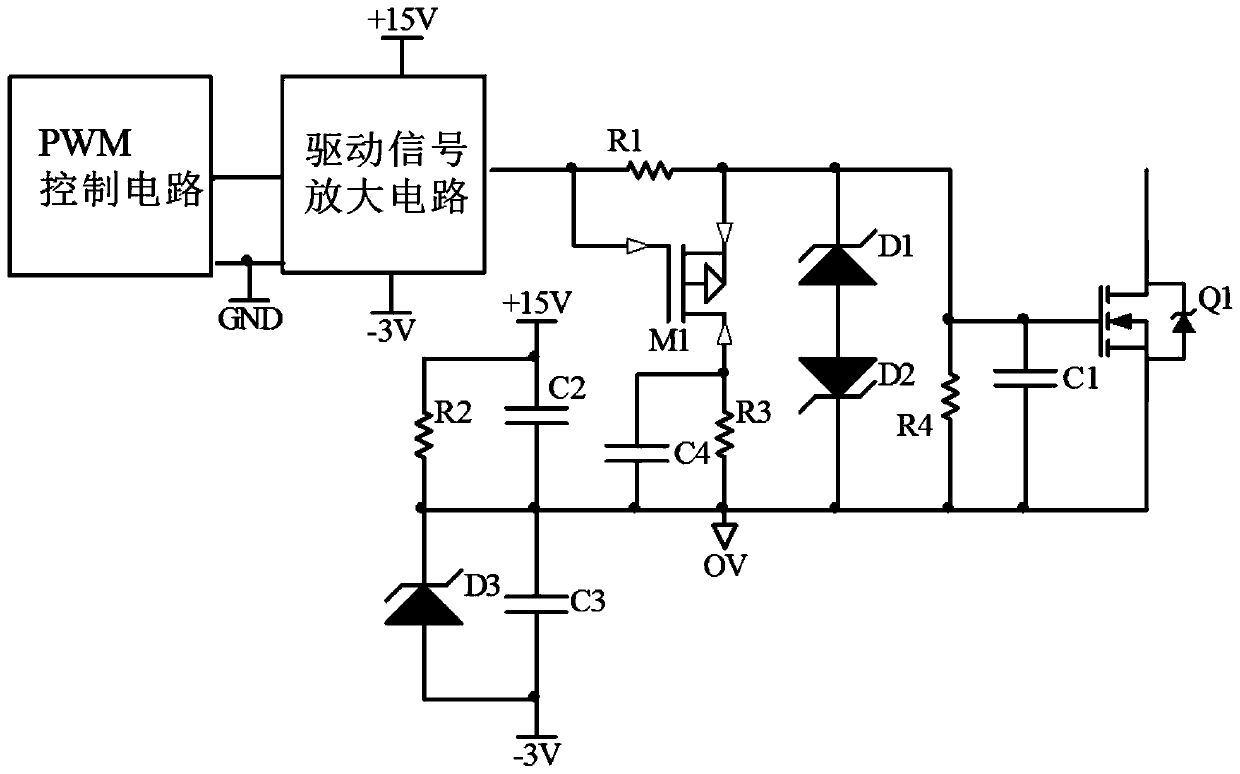
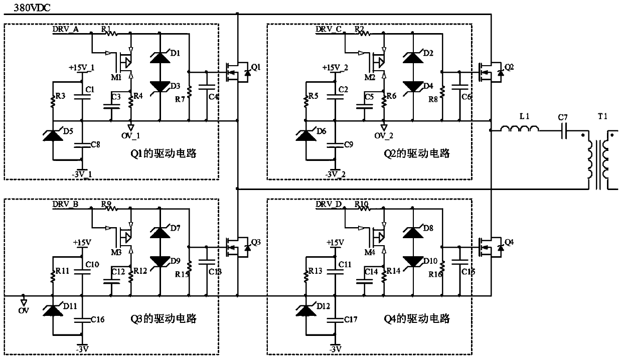
[0017] figure 1 It is the silicon carbide MOSFET driving circuit of the present invention.

[0018] The PWM control circuit generates a PWM pulse signal. After the PWM pulse signal passes through the driving signal amplifier circuit, the silicon carbide MOSFET switch is controlled through the resistor R1. The output of the power supply includes +15V, 0V and -3V DC voltage, and the +15V and -3V DC voltage are respectively given to The driving signal amplification circuit is powered, and 0V is connected to the source of the silicon carbide MOSFET (Q1).

[0019] The driving circuit of Q1 is composed of driving resistor R1, P-channel MOS tube M1, resistor R3, diodes D1, D2, resistor R4 and capacitors C1, C4, the output terminal of the driving signal amplifier circuit is connected with the driving resistor R1 and P-channel MOS tube M1 The gate of M1 is con...


PUM


Abstract

The invention provides a silicon carbide MOSFET driving circuit, which relates to the field of power conversion circuits. A PWM control circuit generates a PWM pulse signal. After the PWM pulse signalpasses through a driving signal amplifying circuit, a silicon carbide MOSFET switch is controlled by a resistor, and a power supply outputs +15V, 0V and -3V DC voltages. The +15V and -3V DC voltagessupply power to the driving signal amplifying circuit, and the 0V is connected to the source of the silicon carbide MOSFET. The silicon carbide MOSFET driving circuit utilizes the driving negative voltage shutdown to reduce crosstalk between the upper and lower tubes of the bridge arm circuit in the power electronic converter, avoiding the bridge arm direct connection, and improving the reliability of the silicon carbide MOSFET; the diode can clamp the gate voltage to a safe range, avoiding breakdown of the silicon carbide MOSFET gate; the circuit uses the MOS transistor M1 to form a dischargeloop, which speeds up the turn-off speed of the silicon carbide MOSFET, improves the switching speed of the silicon carbide MOSFET, and reduces the switching loss.

Description

technical field [0001] The invention relates to the field of power conversion circuits, in particular to a drive circuit applied to power switch tubes. Background technique [0002] Power electronic converters continue to develop in the direction of high frequency, miniaturization and high reliability. High frequency is the development trend of power electronic conversion technology. At present, silicon MOSFETs and IGBTs are widely used in the field of power electronic converters. After decades of application, the performance of ordinary silicon MOSFETs is close to the application limit, which has become one of the main factors restricting the performance of converters. As a new type of power device, silicon carbide MMOSFET has the characteristics of high withstand voltage, high operating temperature, short body diode reverse recovery time, and small parasitic capacitance. Therefore, making full use of the advantages of silicon carbide MOSFET can simplify the converter topol...

Claims


Application Information

Patent Timeline
Patent Type & Authority Patents(China)
IPC IPC(8): H02M1/08H03K17/16H03K17/687
CPCH02M1/08H03K17/161H03K17/687Y02B70/10
Inventor 高田羊彦程泽庄培红
Owner NORTHWESTERN POLYTECHNICAL UNIV
Why Eureka
Try Eureka