A Novel Plasmonic Metamaterial Notched Metasurface

A plasma and metasurface technology, applied in antennas, electrical components, magnetic field/electric field shielding, etc., can solve the problems of difficult spectrum absorption, unfavorable integration and integrated chip manufacturing, complex control circuits, etc., to achieve simple structure and design Flexible, functional effects

Active Publication Date: 2020-04-24
NANJING UNIV OF POSTS & TELECOMM +1
View PDF4 Cites 0 Cited by
  • Summary
  • Abstract
  • Description
  • Claims
  • Application Information

AI Technical Summary

Problems solved by technology

[0003] However, the wave-limiting metasurface in the traditional sense only achieves perfect absorption in a single frequency band, and it is difficult to obtain a tunable absorption spectrum with a certain absorption bandwidth. To obtain such an absorption spectrum, a large number of lumped components have to be introduced , the control circuit is complex and not conducive to integration and chip-based integrated manufacturing

Method used


Image

  • A Novel Plasmonic Metamaterial Notched Metasurface
  • A Novel Plasmonic Metamaterial Notched Metasurface
  • A Novel Plasmonic Metamaterial Notched Metasurface

Examples


Embodiment Construction

[0043] Embodiments of the present invention are described in detail below, examples of which are shown in the drawings, wherein the same or similar reference numerals denote the same or similar elements or elements having the same or similar functions throughout. The embodiments described below by referring to the figures are exemplary only for explaining the present invention and should not be construed as limiting the present invention.

[0044] Those skilled in the art can understand that, unless otherwise defined, all terms (including technical terms and scientific terms) used herein have the same meaning as commonly understood by one of ordinary skill in the art to which this invention belongs. It should also be understood that terms such as those defined in commonly used dictionaries should be understood to have a meaning consistent with the meaning in the context of the prior art, and will not be interpreted in an idealized or overly formal sense unless defined as herein...


PUM


Abstract

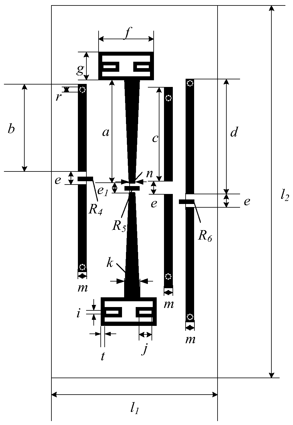
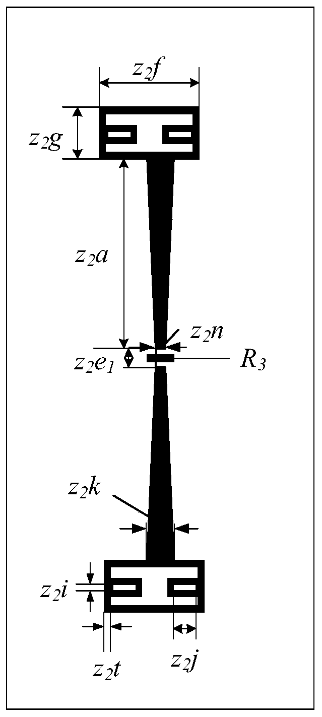
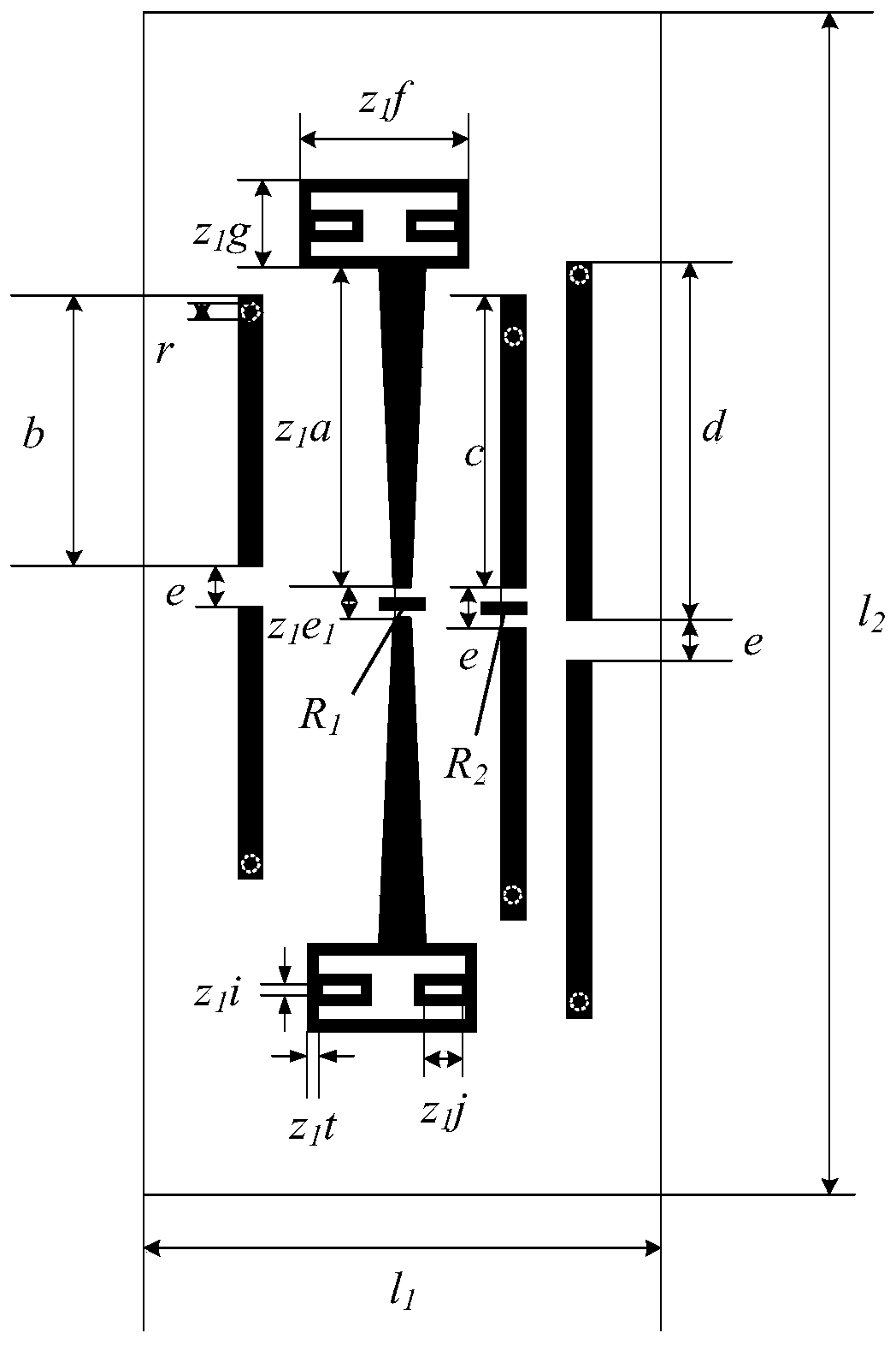
The invention discloses a novel trapped-wave metasurface of a plasma metamaterial. The metasurface comprises a bottom reflecting plate, a dielectric substrate arranged on the reflecting plate, solid-state plasma resonance units arranged on the dielectric substrate, trapezoids and rectangular rings, and six rectangular plasma resonance units arranged at the bottom, wherein the trapezoids and rectangular rings are arranged in the dielectric substrate in an up-down symmetric manner at two layers. Besides, plasma columns are arranged to connect the upper layer and the lower layer; and the plasma at the same layer is connected by resistors. The trapped-wave metasurface can absorb the TE well and reflect the TM eave well. Excitation of different resonance units is realized by controlling excitation areas of the resonance units formed by the solid-state plasma in a programming manner; and ultra-wideband absorption of the TE wave and the reflection of the TM wave by the trapped-wave metasurface can be realized. With the trapped-wave metasurface, absorption of the lower-frequency electromagnetic waves is realized under the small physical size; and polarized separation of the TE wave and theTM wave is realized by the trapped-wave metasurface on the condition of the proper excitation area.

Description

technical field [0001] The invention relates to a novel plasma metamaterial notch metasurface, which belongs to the fields of radio communication and microwave devices. Background technique [0002] With the rapid development of wireless systems and information technology, the electromagnetic environment is becoming more and more complex, and the requirements for anti-interference performance of the system are getting higher and higher. Technology, microwave technology and other fields have broad application prospects. For example, in the military field, the first thing the enemy and the enemy compete for in a war is "electromagnetic control power". The purpose is to control the acquisition and transmission channels of various information on the battlefield, so as to strike each other more effectively and accurately. In terms of life, daily electronic products such as mobile phones, induction cookers, refrigerators, televisions, air conditioners, etc., all have a common fea...

Claims


Application Information

Patent Timeline
Patent Type & Authority Patents(China)
IPC IPC(8): H01Q17/00H05K9/00
CPCH01Q17/00H01Q17/007H05K9/0081
Inventor 章海锋张浩杨靖刘佳轩
Owner NANJING UNIV OF POSTS & TELECOMM
Why Eureka
Try Eureka