


Quick Research
Generate reliable direction feasibility study reports for your R&D in just a few steps.

Technical Q&A
Discover and master advanced knowledge NOW. Basics, ideas, possibilities, all at once.

Find Solutions
As an expert in R&D theories, this can generate solutions to your technical problems instantly.

Evaluate Feasibility
Analyze your overall solution with one click, know your potential R&D risks in advance.

Monitor Landscape
Get weekly tech updates, stay abreast of the latest tech innovations and key insights.
Substrate doping structure and method for forming the same
A technology of substrates and doped regions, applied in semiconductor devices, electrical components, circuits, etc., can solve the problems of increasing the cost of memory technology, and achieve the effect of improving performance and reducing leakage current.
- Summary
- Abstract
- Description
- Claims
- Application Information
AI Technical Summary
Problems solved by technology
Method used
Image

Examples
Embodiment Construction
[0021] The specific implementation of a substrate doping structure and its forming method provided by the present invention will be described in detail below with reference to the accompanying drawings.
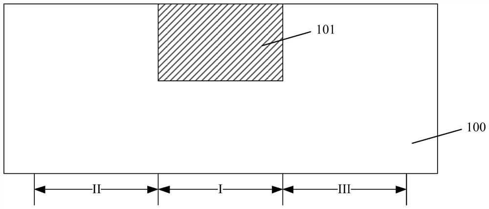
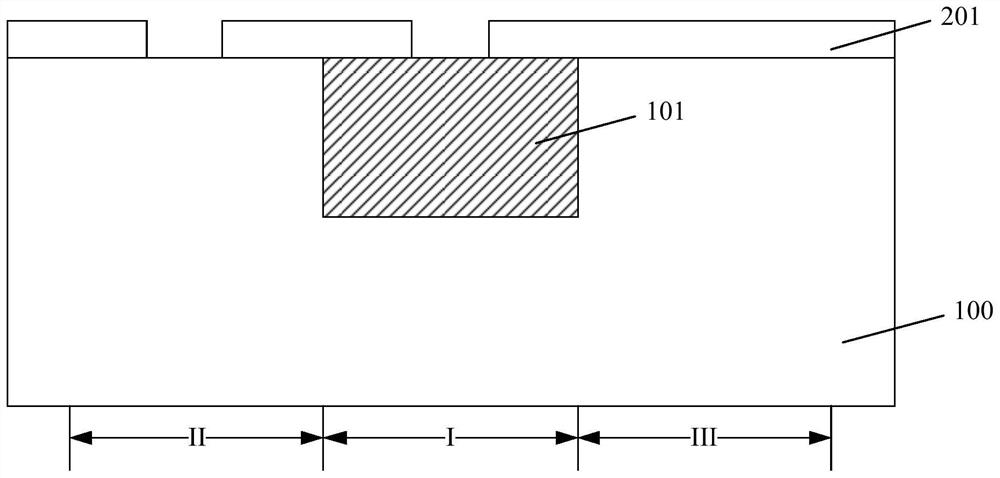
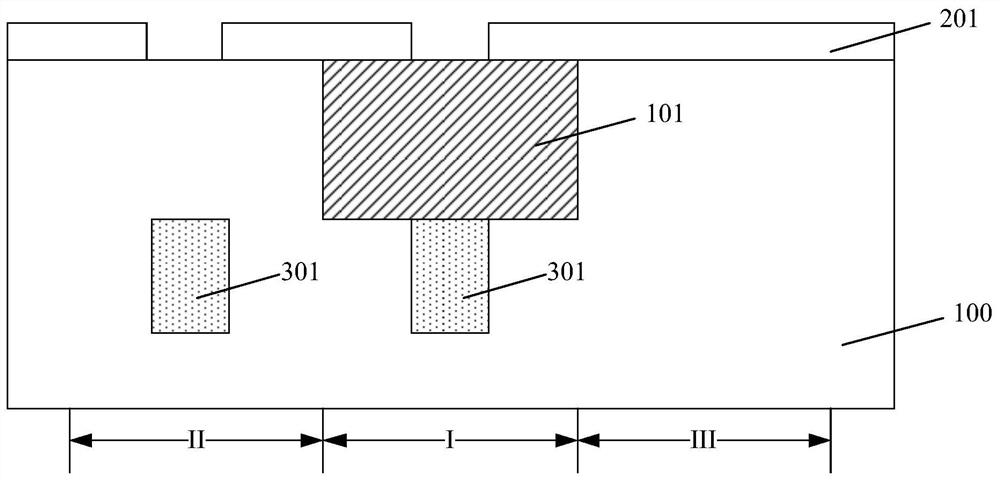
[0022] Please refer to figure 1 , a substrate 100 is provided, and the substrate 100 includes an isolation region I and a first doped well region II.
[0023] The substrate 100 may be a semiconductor material, such as a single-crystal silicon substrate, a single-crystal germanium substrate, an SOI (silicon-on-insulator) or a GOI (germanium-on-insulator) substrate, etc., and the substrate 100 may also be For P-type doping or N-type doping. A person skilled in the art can select a suitable material as the substrate according to actual requirements, which is not limited herein.
[0024] The substrate 100 is used to form a memory, including a storage area and a peripheral circuit area, and the peripheral circuit area is used to form a peripheral circuit to control the memory c...
PUM
 Abstract
Description
Claims
Application Information
 - R&D Engineer
- R&D Manager
- IP Professional
- Industry Leading Data Capabilities
- Powerful AI technology
- Patent DNA Extraction
Browse by: Latest US Patents, China's latest patents, Technical Efficacy Thesaurus, Application Domain, Technology Topic, Popular Technical Reports.
© 2024 PatSnap. All rights reserved.Legal|Privacy policy|Modern Slavery Act Transparency Statement|Sitemap|About US| Contact US: help@patsnap.com