Method for preparing ohmic contact electrode of GaN-base device

A technology for ohmic contact electrodes and devices, which is used in semiconductor/solid-state device manufacturing, semiconductor devices, and electrical solid-state devices. The effect of voltage stabilization

Active Publication Date: 2018-09-28
THE 13TH RES INST OF CHINA ELECTRONICS TECH GRP CORP
View PDF9 Cites 2 Cited by
  • Summary
  • Abstract
  • Description
  • Claims
  • Application Information

AI Technical Summary

Problems solved by technology

[0003] In view of this, an embodiment of the present invention provides a method for preparing a GaN-based device ohmic contact electrode to solve the problem of poor quality of the ohmic contact electrode formed in the prior art

Method used


Image

  • Method for preparing ohmic contact electrode of GaN-base device
  • Method for preparing ohmic contact electrode of GaN-base device

Examples


Embodiment Construction

[0030] In the following description, specific details such as specific system structures and technologies are presented for the purpose of illustration rather than limitation, so as to thoroughly understand the embodiments of the present invention. It will be apparent, however, to one skilled in the art that the invention may be practiced in other embodiments without these specific details. In other instances, detailed descriptions of well-known systems, devices, circuits, and methods are omitted so as not to obscure the description of the present invention with unnecessary detail.

[0031] In order to illustrate the technical solutions of the present invention, specific examples are used below to illustrate.

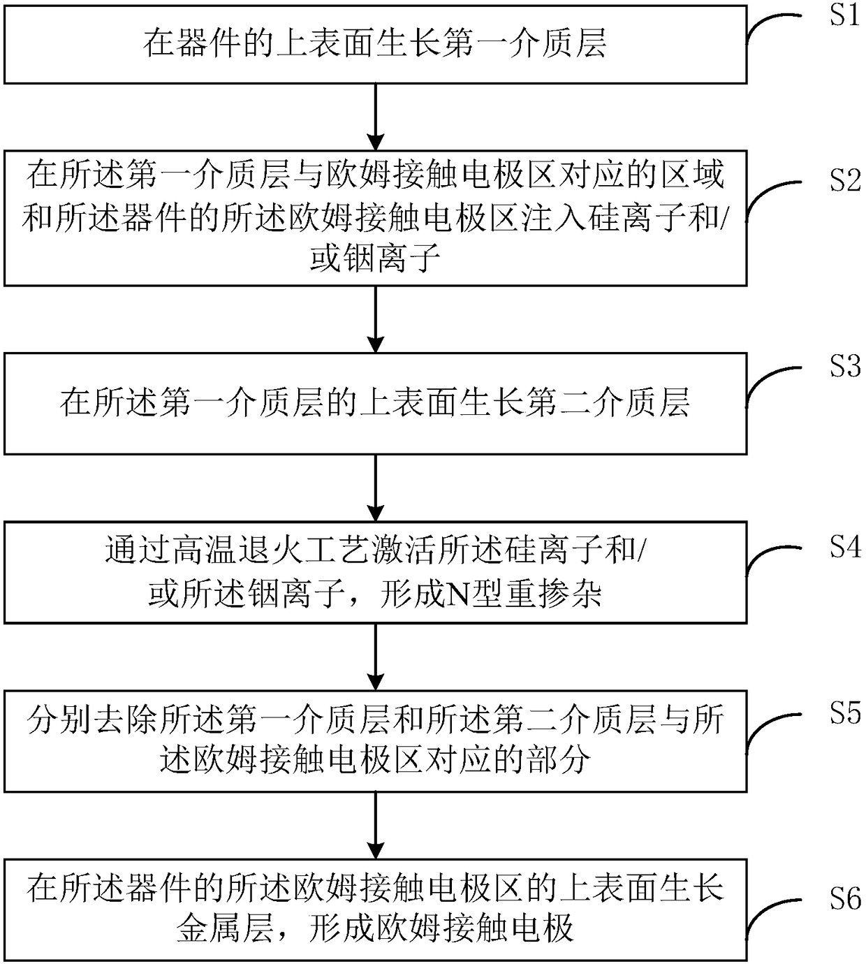
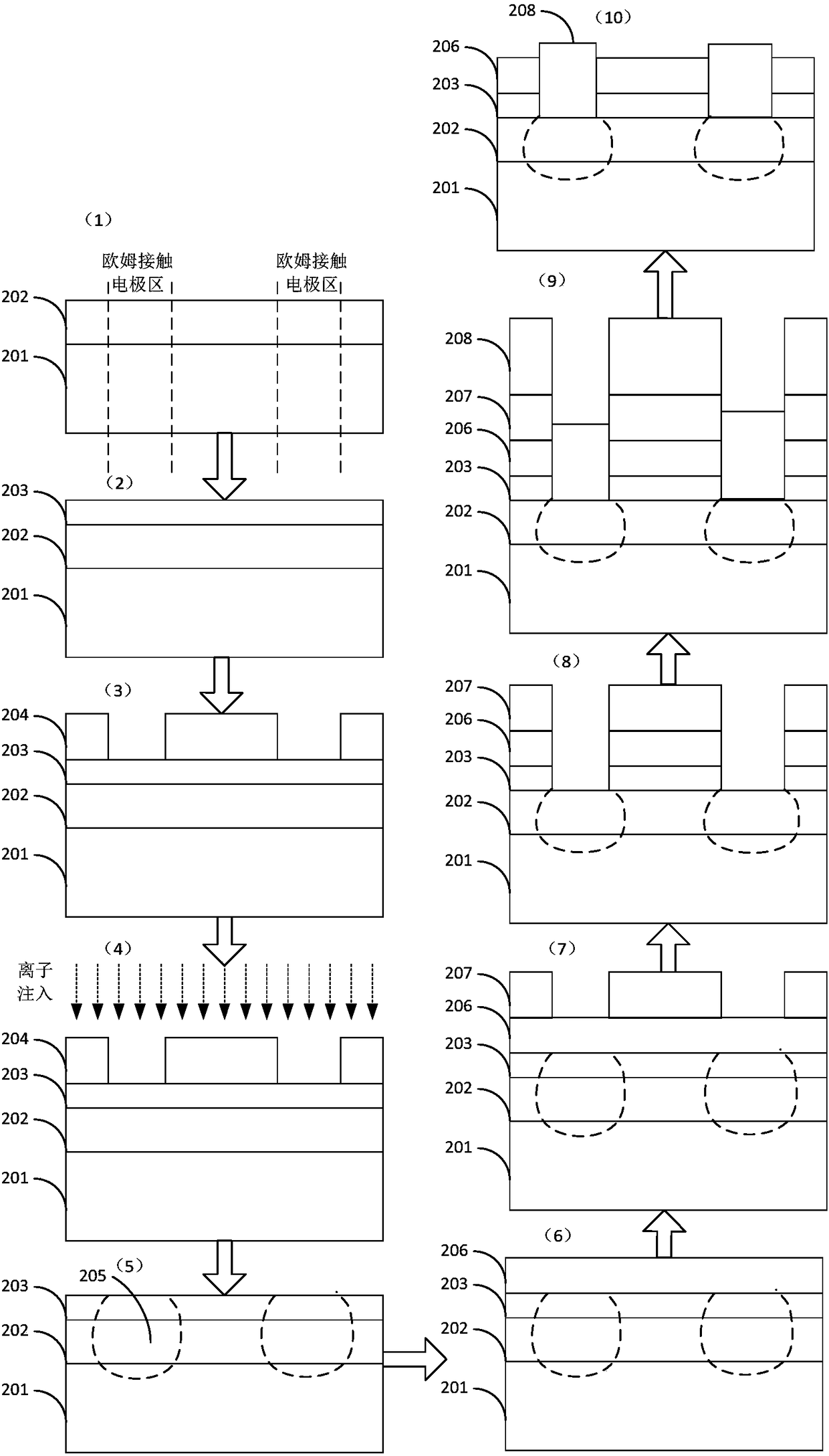
[0032] Please refer to figure 1 , the preparation method of GaN-based device ohmic contact electrode comprises the following steps:

[0033] Step S1, growing a first dielectric layer on the upper surface of the device.

[0034] In the embodiment of the present invent...


PUM


Abstract

The invention is suitable for the field of semiconductors, and provides a method for preparing an ohmic contact electrode of a GaN-base device. The method comprises the following steps: growing a first dielectric layer on the upper surface of a device; injecting silicon ions and/or indium ions in a region, corresponding to an ohmic contact electrode region, of the first dielectric layer and the ohmic contact electrode region of the device; growing a second dielectric layer on the upper surface of the first dielectric layer; activating the silicon ions and/or the indium ions by a high-temperature annealing process, and forming N-type heavy doping; respectively removing the parts, corresponding to the ohmic contact electrode region, of the first dielectric layer and the second dielectric layer; growing a metal layer on the upper surface of the ohmic contact electrode region of the device, and forming the ohmic contact electrode. The prepared ohmic contact electrode can guarantee the flatsurface of the metal layer and the smooth and aligned edges, is stable in breakdown voltage of the device, is high in reliability, and is long in service life.

Description

technical field [0001] The invention belongs to the technical field of semiconductors, and in particular relates to a preparation method of an ohmic contact electrode of a GaN-based device. Background technique [0002] Wide bandgap semiconductor GaN has the advantages of large bandgap width, high two-dimensional electron gas density combined with AlGaN, high breakdown field strength, and high electron saturation drift speed. It has great potential in the field of high-temperature microwave power devices and high-speed power electronic device manufacturing. potential. In GaN-based devices, a good ohmic contact electrode can not only improve the performance of the device, but also help to increase the service life of the device. The traditional method of forming an ohmic contact electrode is to rapidly thermally anneal the metal layer at a temperature higher than 800°C to form an ohmic contact electrode. However, the quality of the ohmic contact electrode formed by this meth...

Claims


Application Information

Patent Timeline
Patent Type & Authority Applications(China)
IPC IPC(8): H01L21/285
CPCH01L21/28575H01L29/452H01L29/2003H01L21/2258H01L21/31116H01L21/31155H01L21/043H01L21/76801H01L23/53295H10K10/84
Inventor 谭永亮吕鑫赵红刚胡泽先崔玉兴付兴昌
Owner THE 13TH RES INST OF CHINA ELECTRONICS TECH GRP CORP
Why Eureka
Try Eureka