High-K dielectric groove lateral double-diffused metal oxide element semiconductor field effect transistor and manufacturing method thereof

A technology of lateral double-diffusion and field effect transistors, applied in the field of lateral double-diffusion metal oxide element semiconductor field effect transistors and its production

Active Publication Date: 2018-09-21
XIDIAN UNIV
View PDF3 Cites 3 Cited by
  • Summary
  • Abstract
  • Description
  • Claims
  • Application Information

AI Technical Summary

Problems solved by technology

In the design optimization process of lateral power devices such as LDMOS, with the optimization of surface electric field terminal technology, including reduced surface electric field technology (Reduced Surface Field, referred to as RESURF), field plate (Field Plate, referred to as FP) technology, lateral variable doping ( With the application of technologies such as Variation of Lateral Doping (VLD for short), the surface electric field of lateral power devices has been optimized to a certain extent, but there are few technologies for optimizing the vertical electric field of devices.

Method used


Image

  • High-K dielectric groove lateral double-diffused metal oxide element semiconductor field effect transistor and manufacturing method thereof

Examples


Embodiment Construction

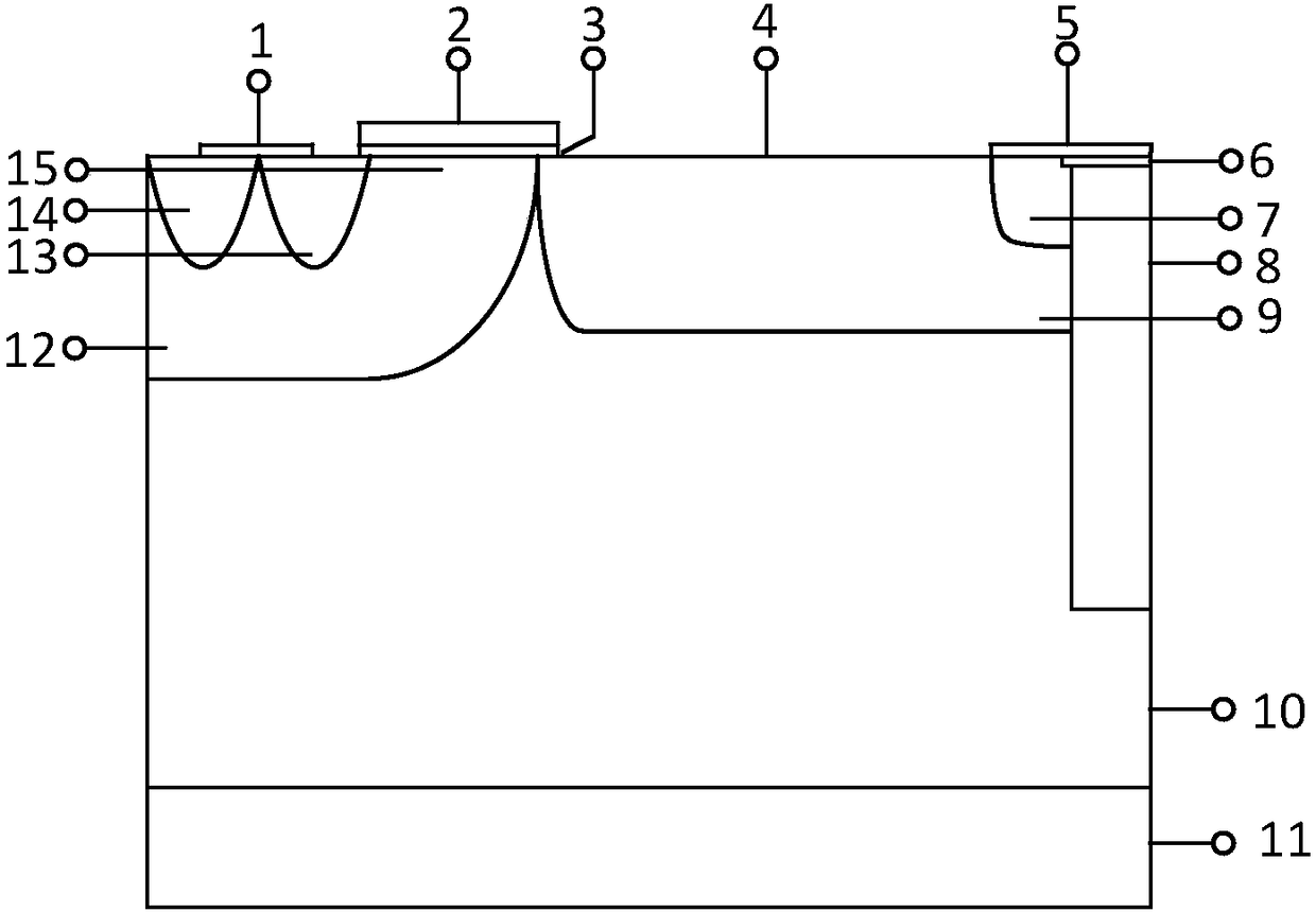
[0043] Such as figure 1 As shown, the high-K dielectric trench lateral double-diffused metal oxide element semiconductor field effect transistor of the present invention includes:

[0044] A substrate 11 of elemental semiconductor material (such as silicon or germanium) (the doping concentration of the substrate is 1×10 13 cm -3 ~1×10 15 cm -3 );

[0045] an epitaxial layer 10 grown on a substrate 11;

[0046] A base region 12 and a drift region 9 formed on the epitaxial layer 10;

[0047] A source region 13 and a channel 15 formed on one side of the base region 12 adjacent to the drift region 9, and a drain region 7 formed on the other side of the drift region 9;

[0048] a channel substrate contact 14 formed outside the source region 13 in the base region;

[0049] The source electrode 1 formed by shorting the contact surface between the source region and the channel substrate;

[0050] A gate insulating layer 3 and a gate electrode 2 formed corresponding to the chan...


PUM


Abstract

The invention provides a high-K dielectric (HK) groove lateral double-diffused metal oxide element semiconductor field effect transistor (LDMOS) and a manufacturing method thereof. According to the device, a deep groove high dielectric constant dielectric layer is formed on the drain end, the lower end of the high-K dielectric groove layer goes deep into the epitaxial layer arranged on the substrate of the device and the upper end is connected with the drain electrode of the device. The HK dielectric groove and the element semiconductor material substrate form an MIS capacitor structure, and the charges of the substrate of the device can be auxiliarily exhausted when the device is turned off so that the LDMOS having the low resistance substrate is enabled to acquire high breakdown voltage.Besides, the electric field distribution in the device body can be effectively modulated by the uniform electric field of the HK dielectric groove in case of device reverse voltage withstanding so that the longitudinal high electric field of the drain end of the device can be reduced, the breakdown voltage of the device can be enhanced and the problem of saturation of the breakdown voltage of theLDMOS along with increasing of the length of the drift region can be solved.

Description

technical field [0001] The invention relates to the field of power semiconductor devices, in particular to a lateral double-diffusion metal oxide element semiconductor field effect transistor and a manufacturing method thereof. Background technique [0002] With the rapid development of new power semiconductor devices represented by power MOSFET devices, power semiconductor devices are widely used in computer, lighting, consumer electronics, automotive electronics, industrial drives and other fields. Power semiconductor devices are the core of green, low power consumption, energy saving and environmental protection device. Lateral Double-diffused MOS (Lateral Double-diffused MOS, referred to as LDMOS) as a representative of the lateral power device with high withstand voltage and low on-resistance has the advantages of easy integration, good thermal stability, good frequency stability, low power consumption, The advantages of multi-element conduction, small power drive, and...

Claims


Application Information

Patent Timeline
IPC IPC(8): H01L29/78H01L29/08H01L29/06H01L21/336
CPCH01L29/0611H01L29/0886H01L29/66681H01L29/7816
Inventor 段宝兴曹震董自明师通通杨银堂
Owner XIDIAN UNIV
Why Eureka
Try Eureka