Design method for heterogeneous reconfigurable diagram calculation accelerator system on the basis of FPGA (Field Programmable Gate Array)

A design method and accelerator technology, applied in computer-aided design, CAD circuit design, calculation, etc., can solve the problems of low software level, low effective calculation rate, low utilization rate of off-chip bandwidth, etc., to achieve low power consumption, acceleration The effect of graph algorithms

Active Publication Date: 2018-09-21
UNIV OF SCI & TECH OF CHINA
View PDF2 Cites 27 Cited by
  • Summary
  • Abstract
  • Description
  • Claims
  • Application Information

AI Technical Summary

Problems solved by technology

In the design and implementation of graph computing systems at the software level, there are often some inefficient and unavoidable problems at the software level, such as low utilization of off-chip bandwidth and low effective computing rate.

Method used


Image

  • Design method for heterogeneous reconfigurable diagram calculation accelerator system on the basis of FPGA (Field Programmable Gate Array)
  • Design method for heterogeneous reconfigurable diagram calculation accelerator system on the basis of FPGA (Field Programmable Gate Array)
  • Design method for heterogeneous reconfigurable diagram calculation accelerator system on the basis of FPGA (Field Programmable Gate Array)

Examples


Embodiment

[0055] FPGA in the embodiment of the present invention refers to Field Programmable Gate Arrays (Field Programmable GateArrays), and the system designed in the present invention is a heterogeneous system based on PC-FPGA, wherein, the data path between PC and FPGA can adopt PCI-E bus protocol. The data path inside the FPGA on-chip accelerator is illustrated by using the AXI bus protocol as an example to illustrate the data path in the drawings of the embodiments of the present invention, but the present invention is not limited thereto.

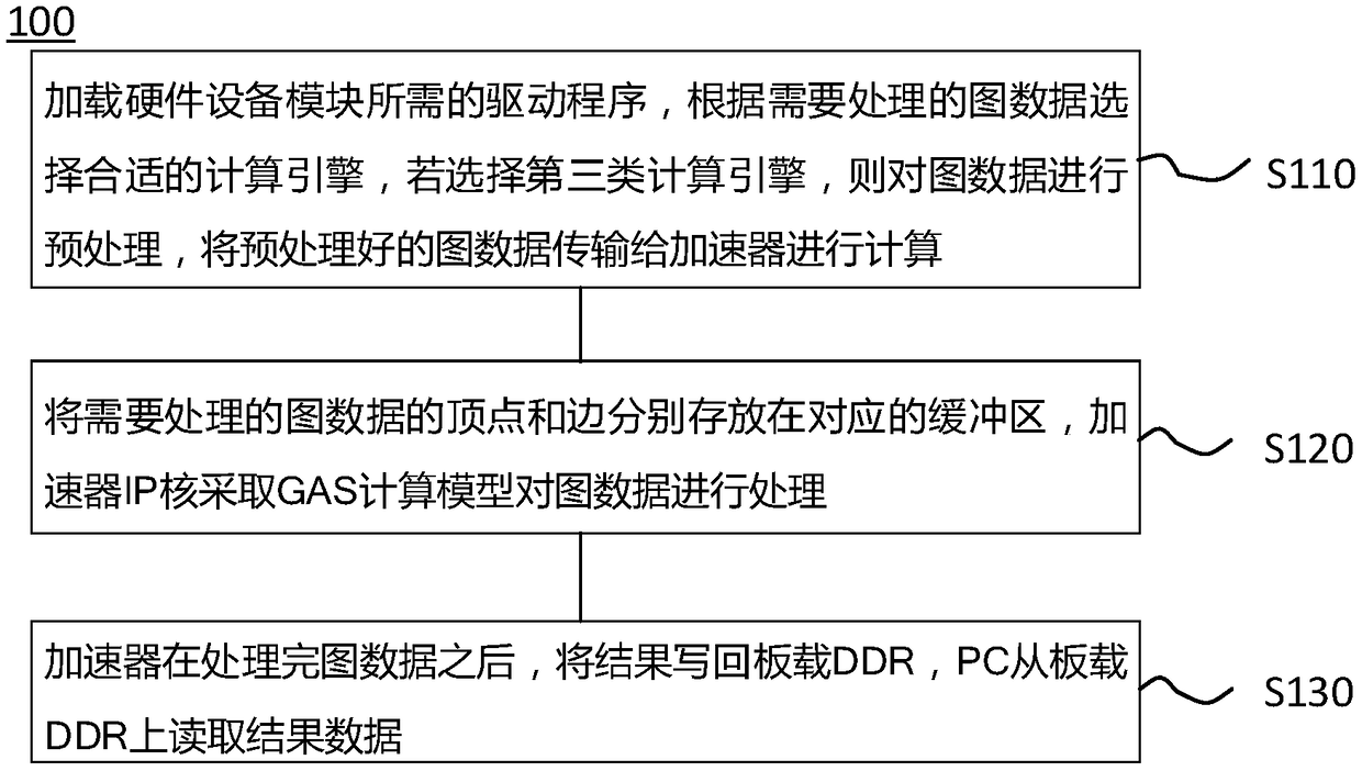
[0056] figure 1 It is a flowchart of an FPGA-based graph computing accelerator design method 100 according to an embodiment of the present invention. The method 100 includes:

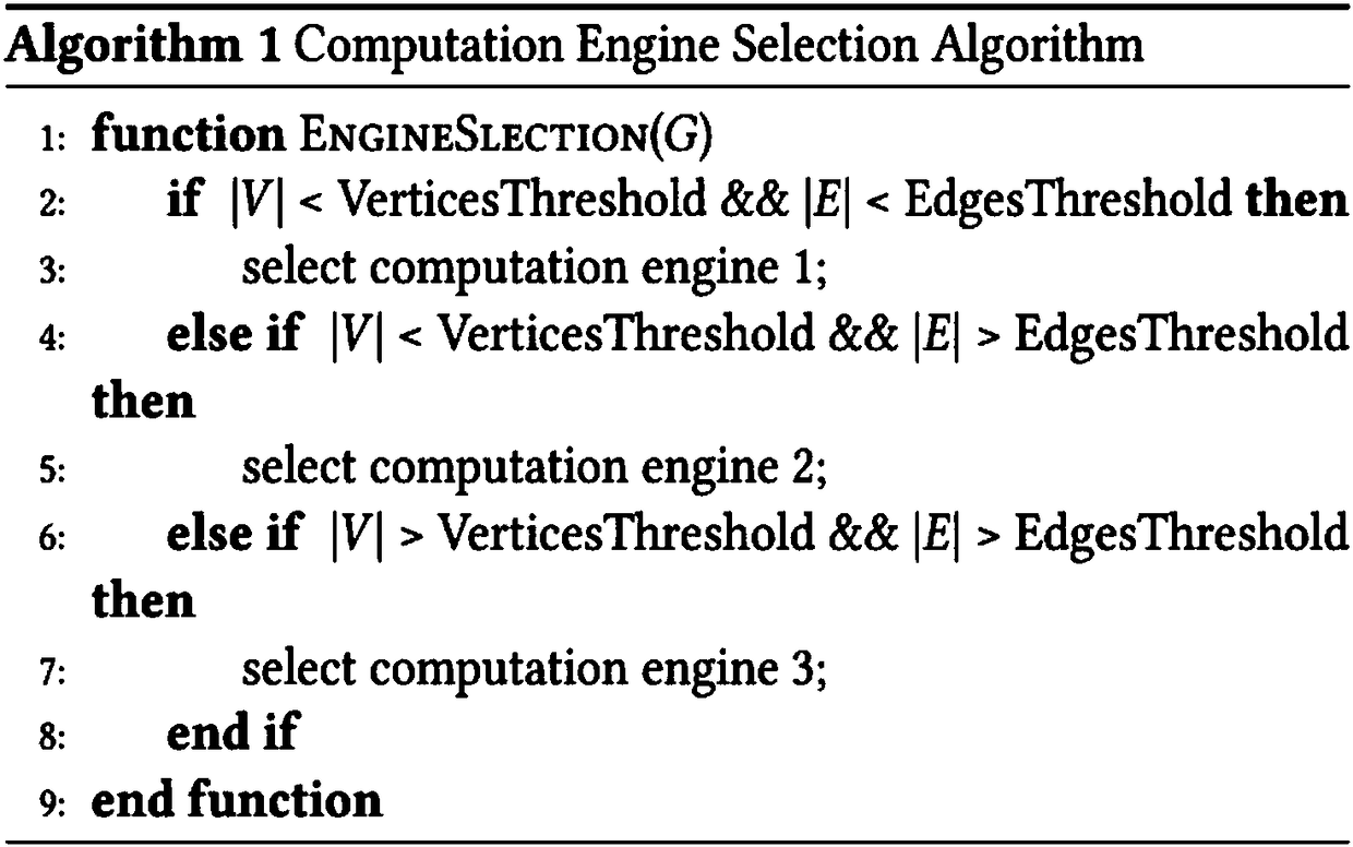
[0057] S110, load the driver program required by the hardware device module, select a suitable computing engine according to the graph data to be processed, if the third type of computing engine is selected, preprocess the graph data, and transmit the preprocessed gr...


PUM


Abstract

The invention discloses a design method for a heterogeneous reconfigurable diagram calculation accelerator system on the basis of an FPGA (Field Programmable Gate Array). A whole accelerator system comprises a PC (Personal Computer) heterogeneous module and an FPGA heterogeneous module. The design method comprises the following specific steps that: firstly, loading a driving module required for starting the FPGA, and starting equipment, including the PCIe (Peripheral Component Interface Express) DMA (Direct Memory Access) and the like of the FPGA; according to the vertex number and the edge number of diagram data which needs to be processed, selecting a diagraph calculation accelerator engine; preprocessing the diagram data after the accelerator engine is selected; transmitting the processed diagram data to the onboard DDR (Double Data Rate) of an FPGA development board through the PCIe DMA; starting the accelerator to begin to read graph data from the appointed address of the onboardDDR; distributing the graph data to different processing units to be processed and calculated by the controller; after each processing unit calculates and processes the data, sending a result to a calculation result collection module; and writing the result back to the onboard DDR by the collection module, and reading the result from the onboard DDR by the PC after the whole diagram data finishesbeing processed. The method has the characteristics of being high in performance, energy efficiency, power consumption and the like.

Description

technical field [0001] The invention relates to the field of computer hardware acceleration, in particular to an FPGA-based graph computing accelerator system design method. Background technique [0002] In the real world, a graph can be used to represent the relationship between different entities. It is an abstraction of the relationship model between entities. A lot of information can be stored in the graph structure, so it has a wide range of applications in practice, such as: social network Analysis, web page map search, product recommendation system establishment, traffic network analysis, and biomedical information analysis, etc. In today's era of big data, the scale of graphs is becoming larger and larger. For example, the number of Facebook users reached 2.2 billion in July 2014, and the number of relationships between users reached hundreds or even hundreds of billions. If the relationship between these users Stored in the form of graph edges, the storage capacity...

Claims


Application Information

Patent Timeline
Patent Type & Authority Applications(China)
IPC IPC(8): G06F17/50
CPCG06F30/331G06F2117/08
Inventor 周学海李曦王超陈香兰
Owner UNIV OF SCI & TECH OF CHINA
Why Eureka
Try Eureka