Mask plate and manufacturing method thereof

A manufacturing method and mask technology, applied in semiconductor/solid-state device manufacturing, ion implantation plating, coating, etc. It can achieve 25μm to 40μm and other problems, achieving the effect of high quality and precision, reducing thickness and improving quality

Active Publication Date: 2018-09-18
NINGBO SEMICON INT CORP
View PDF5 Cites 13 Cited by
  • Summary
  • Abstract
  • Description
  • Claims
  • Application Information

AI Technical Summary

Problems solved by technology

[0004] At present, the metal mask plate of OLED (Organic Light-Emitting Diode, organic light-emitting display) is usually made of Invar alloy (INVAR, also known as Invar) with a thickness of 30 μm to 50 μm and is prepared by chemical etching. The surface of the alloy is coated with photoresist or photosensitive dry film, and the fine pattern of the mask plate is transferred to the photosensitive film by exposure, and then a fine metal mask plate is made by developing and chemical etching. The precision is usually at the micron level, and generally the minimum can only be 25 μm to 40 μm, so the quality and accuracy of the metal mask produced cannot well meet the process requirements

Method used


Image

  • Mask plate and manufacturing method thereof
  • Mask plate and manufacturing method thereof
  • Mask plate and manufacturing method thereof

Examples


Embodiment Construction

[0017] It can be seen from the background technology that the quality and accuracy of the metal mask cannot well meet the requirements of the process.

[0018] In order to solve the technical problem, the present invention uses semiconductor processes such as deposition, photolithography and etching to make a mask. Compared with the metal mask made by traditional chemical etching, the semiconductor process can improve the The quality of the mask plate and the accuracy of the through holes are improved, thereby improving the quality and accuracy of the mask plate, which is beneficial to improving the precision of the evaporation process.

[0019] In order to make the above objects, features and advantages of the present invention more comprehensible, specific embodiments of the present invention will be described in detail below in conjunction with the accompanying drawings.

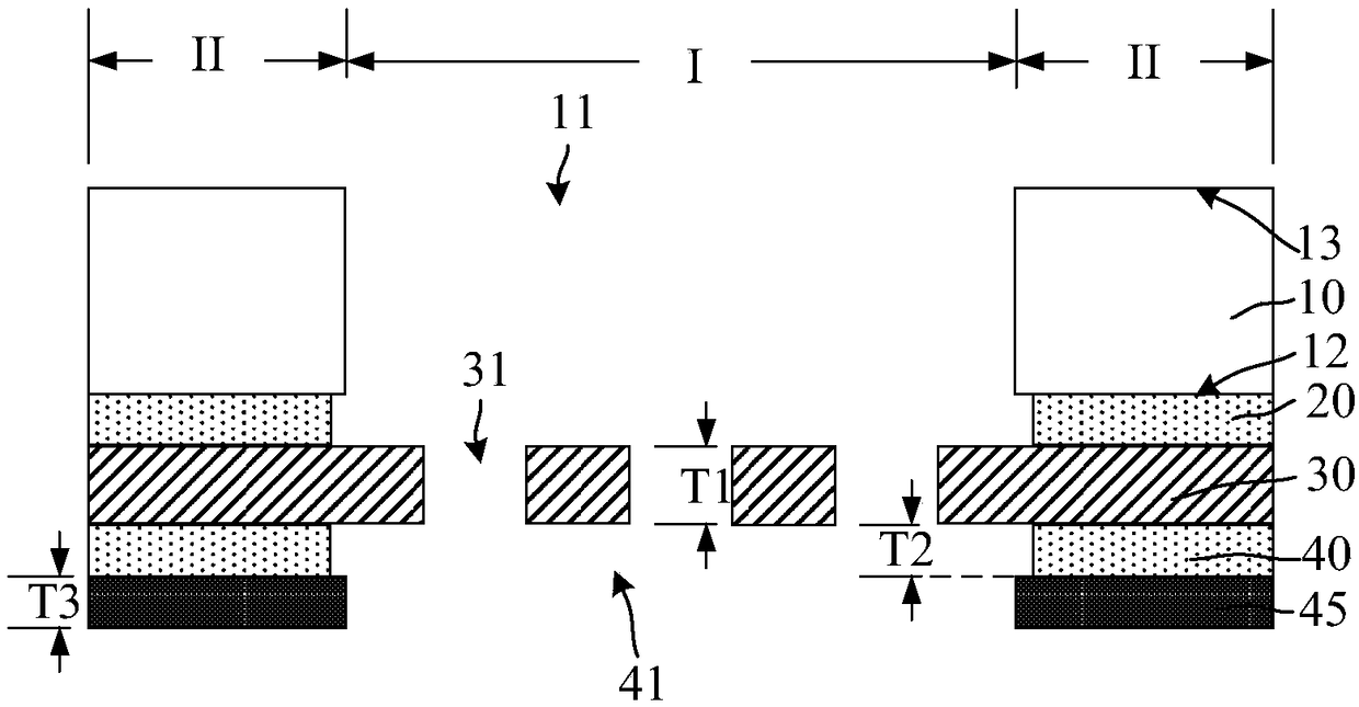
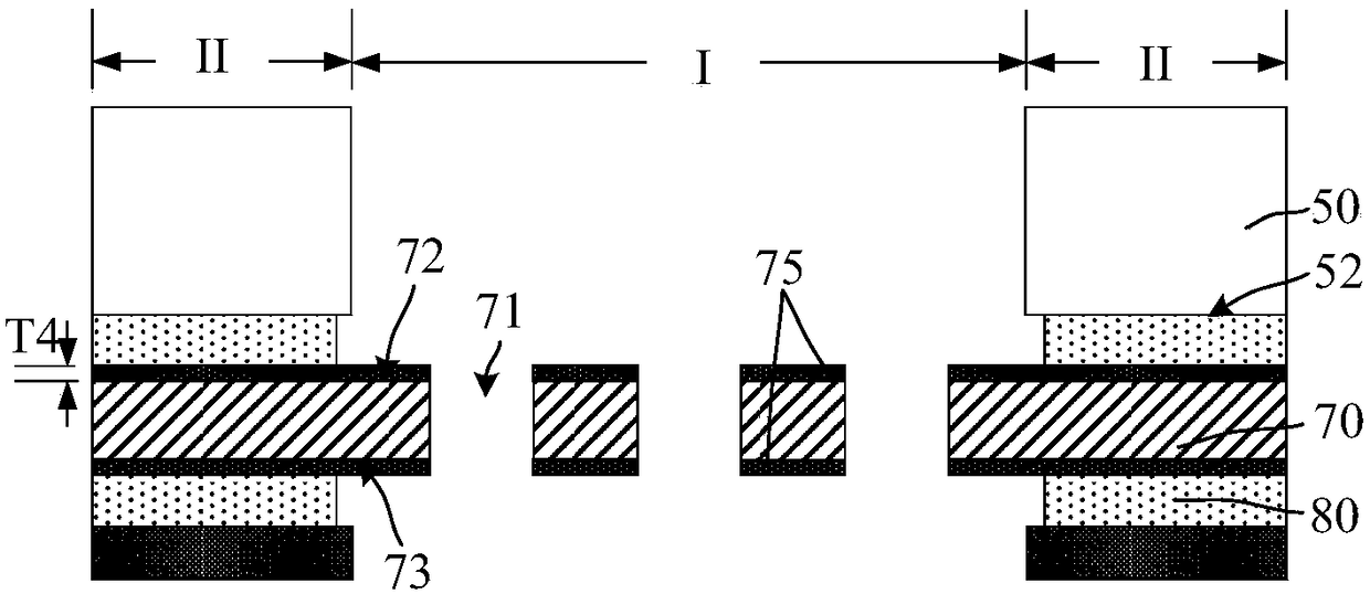
[0020] figure 1 It is a structural schematic diagram of an embodiment of the mask plate of the presen...


PUM


Abstract

The invention discloses a mask plate and a manufacturing method of the mask plate. The mask plate comprises a substrate, a mask graph layer, a protection layer and a first sacrificial layer. The substrate comprises a first surface and a second surface reverse to the first surface, multiple openings penetrating the substrate are formed in the substrate, the substrate can use the semiconductor etching process to carry out imaging, the mask graph layer is located on the first surface and comprises a graph area and a shielding area which are adjacent, the graph area is provided with at least one through hole penetrating the mask graph layer, the openings are exposed out of the graph area, each graph area corresponds to the openings, the protection layer is located at the position, on the side,back onto the substrate, of the mask graph layer, of the surface of the shielding area, and the first sacrificial layer is located between the mask graph layer and the protection layer. The mask plate is made through the semiconductor process, compared with a metal mask plate made through the traditional chemical etching manner, the semiconductor process can improve the quality of the mask plateand the through hole precision, the through hole size is reduced, the mask graph layer thickness is reduced, the mask graph layer and the substrate can be prevented from shifting, and the mask plate quality and the precision are higher.

Description

technical field [0001] The invention relates to the field of semiconductor manufacturing, in particular to a mask plate and a manufacturing method thereof. Background technique [0002] Physical vapor deposition (Physical Vapor Deposition, PVD) technology is mainly divided into two types: evaporation (Evaporation) process and sputtering (Sputtering) process. Among them, the evaporation process is the main way to form a functional film layer on the surface of the substrate. The evaporation process refers to heating and melting the evaporation source (such as metal, alloy or compound to be plated) in a vacuum evaporation machine (Vacuum Evaporator), so that It escapes in the form of molecules or atoms, and is deposited on the surface of the substrate to form a solid film or coating. [0003] At present, the evaporation process mainly adopts a metal mask (Metal Mask), and the metal mask has a predetermined pattern of through holes. During the evaporation process, the metal mas...

Claims


Application Information

Patent Timeline
IPC IPC(8): C23C14/04H01L51/56
CPCC23C14/04H10K71/00
Inventor 刘孟彬罗海龙
Owner NINGBO SEMICON INT CORP
Why Eureka
Try Eureka