CMOS digital integration circuit board manufacturing process

A manufacturing process and circuit board technology, used in circuits, semiconductor/solid-state device manufacturing, electrical components, etc., can solve problems such as reducing parasitic capacitance, not completely ensuring that different conductive layers are insulated from each other, and unable to accurately control channel length, etc. Good isolation effect

Inactive Publication Date: 2018-09-04
南浔双林荣丰磁材厂
View PDF1 Cites 0 Cited by
  • Summary
  • Abstract
  • Description
  • Claims
  • Application Information

AI Technical Summary

Problems solved by technology

[0003] The current manufacturing process of CMOS digital integrated circuit boards cannot activate impurities and make impurities reach deep distribution at the same time; the isolation effect between devices is poor; the gate connection between NMOS and PMOS is inconvenient; the channel length cannot be accurately controlled. Parasitic capacitance and the inability to completely guarantee the mutual isolation between different conductive layers

Method used


Image

  • CMOS digital integration circuit board manufacturing process

Examples


Embodiment Construction

[0021] The following will clearly and completely describe the technical solutions in the embodiments of the present invention with reference to the accompanying drawings in the embodiments of the present invention. Obviously, the described embodiments are only some, not all, embodiments of the present invention. Based on the embodiments of the present invention, all other embodiments obtained by persons of ordinary skill in the art without making creative efforts belong to the protection scope of the present invention.

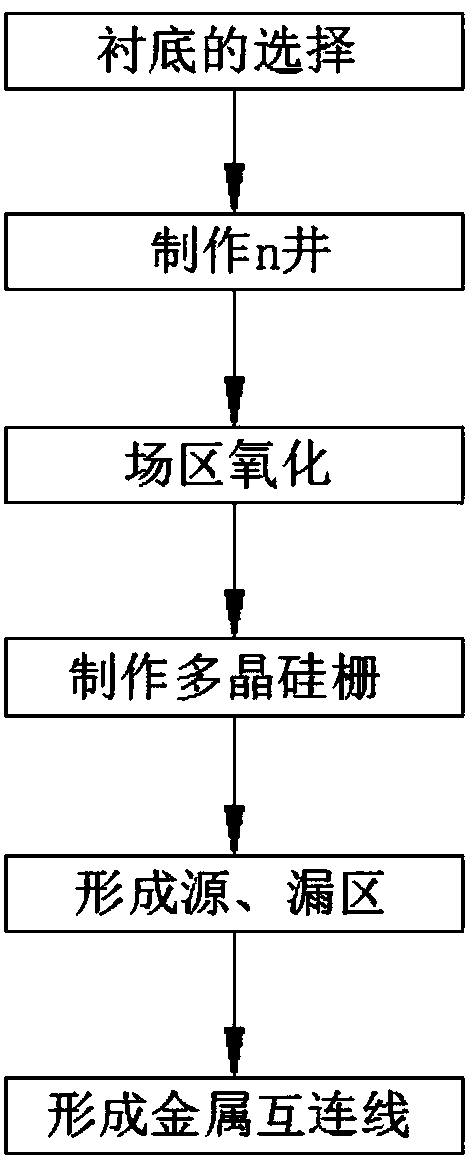
[0022] see figure 1 , the invention provides a technical solution: a manufacturing process of a CMOS digital integrated circuit board, comprising the following steps:

[0023] S1. Selection of the substrate: select an epitaxial silicon wafer with a small substrate resistivity but with an epitaxial layer as the substrate;

[0024] S2. Fabrication of n-well: First, thermally oxidize the original silicon wafer to form a masking layer for implantation in the well...


PUM


Abstract

The present invention discloses a CMOS digital integration circuit board manufacturing process. The manufacturing process comprises the following steps of: S1, selection of a substrate; S2, manufacturing of an n well; S3, oxidation of court areas; S4, manufacturing of a polysilicon gate; S5, formation of a source region and a drain region; S6, formation of a metal interaction wire; and S7, coverage of a layer of phosphorosilicate glass passive film on a silicon wafer after formation of the metal interaction wire to perform once photoetching to expose a leading-out terminal and pressure pointsof a silicon wafer of the integration circuit and connect the pressure points of the silicon wafer and corresponding pins of a tube.

Description

technical field [0001] The invention relates to the technical field of integrated circuit boards, in particular to a manufacturing process of CMOS digital integrated circuit boards. Background technique [0002] CMOS digital integrated circuit board is a complementary circuit composed of PMOS and NMOS. PMOS needs an n-type substrate, and NMOS needs a p-type substrate. In a CMOS circuit, PMOS and NMOS should be fabricated on one substrate. The CMOS circuit solves this problem by making a well. According to the structure, CMOS circuits can be divided into three types: n-well CMOS, p-well CMOS and double-well CMOS. [0003] The current manufacturing process of CMOS digital integrated circuit boards cannot activate impurities and make impurities reach deep distribution at the same time; the isolation effect between devices is poor; the gate connection between NMOS and PMOS is inconvenient; the channel length cannot be accurately controlled. Parasitic capacitance and the inabil...

Claims


Application Information

Patent Timeline
Patent Type & Authority Applications(China)
IPC IPC(8): H01L21/8238
CPCH01L21/8238H01L21/823807H01L21/823871H01L21/823878H01L21/823892
Inventor 沈利明
Owner 南浔双林荣丰磁材厂
Why Eureka
Try Eureka