Inorganic full-solid-state electrochromic device with quick responsiveness and preparation method
An electrochromic device, all-solid-state technology, applied in instruments, nonlinear optics, optics, etc., can solve problems such as uneven distribution of electric field, long discoloration time, uneven discoloration, etc., to improve the distribution of electric field and voltage, improve Effect of uneven discoloration and improvement of discoloration response time
- Summary
- Abstract
- Description
- Claims
- Application Information
AI Technical Summary
Problems solved by technology
Method used
Image
Examples
preparation example Construction
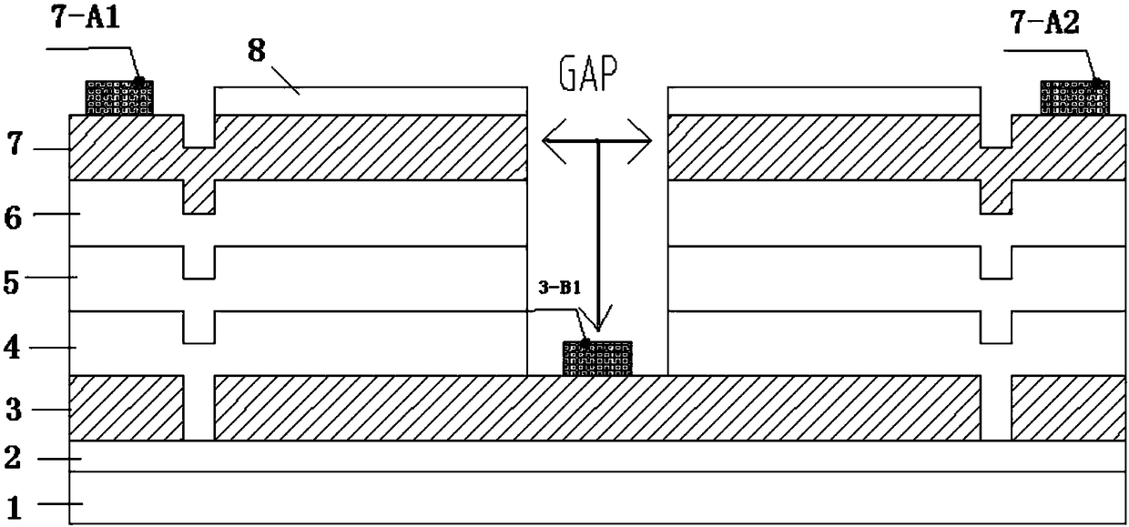
[0055] Correspondingly, an embodiment of the present invention provides a method for preparing an inorganic all-solid-state electrochromic device as described above, including the following steps:
[0056] On the substrate, a bottom protective layer and a bottom conductor layer are sequentially formed by vapor deposition, and the bottom conductor layer is not short-circuited;
[0057]On the bottom conductor layer, a color-changing layer, a conduction layer, a storage layer and a top conductor layer are sequentially formed by vapor deposition, and the top conductor layer is not short-circuited;
[0058] Using a laser to penetrate from the top conductor layer to the bottom conductor layer to form several cavity trenches, so that the top conductor layer is divided into multiple units;
[0059] An electrode is independently fabricated on each unit of the top conductor layer, and an intermediate electrode is fabricated on the bottom conductor layer corresponding to at least one cav...
Embodiment 1
[0074] Example 1: Preparation of dichromatic region devices
[0075] (1) The glass substrate (thickness 1.6mm, transmittance 92%, flatness 1.5%) is washed and dried, and enters the coating system.
[0076] (2) Sputtering rotating silicon target to prepare silicon dioxide; set power AC 30KW, atmosphere: argon and oxygen mixed, air pressure 3×10 -4 mbar, film thickness 15nm.
[0077] (3) Magnetron sputtering rotating indium tin oxide target to prepare indium tin oxide conductor layer; DC pulse power supply, power DC60KW, argon sputtering, air pressure 5×10 -4 mbar, film thickness 150nm.
[0078] In the atmospheric environment, the conductor layer is cut and scribed by laser etching P1, so that the conductor layer has two gaps on the left and right to avoid the bottom ITO short circuit; the gap width is 0.5mm.
[0079] (4) Radio frequency reactive sputtering to prepare a tungsten oxide layer; a metal tungsten target is used to make a tungsten oxide layer by radio frequency rea...
Embodiment 2
[0090] Example 2: Preparation of four-color-changing region devices
[0091] (1) The glass substrate (thickness 2.2mm, transmittance 92%, flatness 1.5%) is cleaned and dried, and enters the coating system.
[0092] (2) Sputtering rotating silicon target to prepare silicon dioxide; set power AC 30KW, atmosphere: argon and oxygen mixed, air pressure 3×10 -4 mbar, film thickness 15nm.
[0093] (3) Magnetron sputtering rotating indium tin oxide target to prepare indium tin oxide conductor layer; DC pulse power supply, power DC60KW, argon sputtering, air pressure 5×10 -4 mbar, film thickness 150nm.
[0094] In the atmospheric environment, the conductor layer is cut and scribed by laser etching P1, so that the conductor layer has two gaps on the left and right to avoid the bottom ITO short circuit; the gap width is 0.5mm.
[0095] (4) Radio frequency reactive sputtering to prepare a tungsten oxide layer; a metal tungsten target is used to make a tungsten oxide layer by radio freq...
PUM
| Property | Measurement | Unit |
|---|---|---|
| width | aaaaa | aaaaa |
| width | aaaaa | aaaaa |
| width | aaaaa | aaaaa |
Abstract
Description
Claims
Application Information
 - R&D
- Intellectual Property
- Life Sciences
- Materials
- Tech Scout
- Unparalleled Data Quality
- Higher Quality Content
- 60% Fewer Hallucinations
Browse by: Latest US Patents, China's latest patents, Technical Efficacy Thesaurus, Application Domain, Technology Topic, Popular Technical Reports.
© 2025 PatSnap. All rights reserved.Legal|Privacy policy|Modern Slavery Act Transparency Statement|Sitemap|About US| Contact US: help@patsnap.com


