
Mass transfer device and transfer method of miniature light-emitting diode

A technology of light-emitting diodes and transfer devices, which is applied in transportation and packaging, electrical components, semiconductor/solid-state device manufacturing, etc., can solve problems that hinder the promotion and use of micro-light-emitting diode technology, and achieve high yield, low cost, and simple process Effect

Pending Publication Date: 2018-08-28
QUANZHOU SHENGWEI ELECTRONICS TECH CO LTD
View PDF12 Cites 33 Cited by
  • Summary
  • Abstract
  • Description
  • Claims
  • Application Information

AI Technical Summary

Problems solved by technology

Since mass transfer technology requires very high efficiency, yield rate and transfer accuracy, mass transfer technology has become the biggest challenge in the research and development process of micro-LEDs, hindering the promotion and use of micro-LED technology

Method used


Image

  • Mass transfer device and transfer method of miniature light-emitting diode
  • Mass transfer device and transfer method of miniature light-emitting diode
  • Mass transfer device and transfer method of miniature light-emitting diode

Examples


Embodiment Construction

[0040] The following describes several preferred embodiments of the present invention with reference to the accompanying drawings, so as to make the technical content clearer and easier to understand. The present invention can be embodied in many different forms of embodiments, and the protection scope of the present invention is not limited to the embodiments mentioned herein.

[0041] In the drawings, components with the same structure are denoted by the same numerals, and components with similar structures or functions are denoted by similar numerals. The size and thickness of each component shown in the drawings are shown arbitrarily, and the present invention does not limit the size and thickness of each component. In order to make the illustration clearer, the thickness of parts is appropriately exaggerated in some places in the drawings.

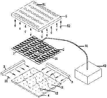
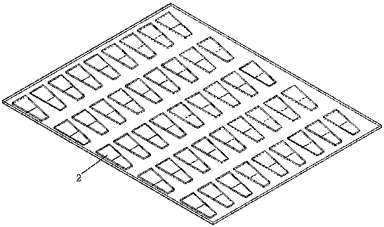
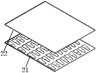
[0042] Such as figure 1As shown, a mass transfer device for micro-LEDs includes a micro-LED array groove plate 1 and a micro-LED e...


PUM


Abstract

The invention discloses a mass transfer device and transfer method of a miniature light-emitting diode, and relates to the field of light-emitting display. The mass transfer device comprises a miniature light-emitting diode array groove plate (1) and a miniature light-emitting diode component (2), wherein the miniature light-emitting diode component (2) is placed in a miniature light-emitting diode groove (11) of the miniature light-emitting diode array groove plate (1), a horizontal air blowing device (3) and a vertical air blowing and oscillation device (4) are arranged below the miniature light-emitting diode array groove plate (1), a detection device (5) is arranged above the miniature light-emitting diode array groove plate (1), the miniature light-emitting diode array groove plate (1) comprises a substrate layer (100), a driving circuit layer (101) and a protection layer (102). By the mass transfer device and transfer method of the miniature light-emitting diode, no transfer toolis needed, and simple process, high yield, high transfer accuracy and low cost are achieved.

Description

technical field [0001] The invention relates to the field of light-emitting display, in particular to a mass transfer device and transfer method of micro light-emitting diodes. Background technique [0002] Micro light-emitting diode (Micro LED) is a display technology that miniaturizes and matrixes the traditional LED structure, and uses CMOS integrated circuit technology to make a driving circuit to realize the addressing control and individual driving of each pixel. Since the brightness, life, contrast, response time, energy consumption, viewing angle and resolution of micro light-emitting diodes are stronger than those of LCD and OLED technologies, and they are self-illuminating, simple in structure, small in size and energy-saving. Advantages, it has been regarded as the next generation of display technology by many manufacturers and has begun to actively deploy it. A core technical problem faced by micro-LEDs in the process of industrialization is the Mass Transfer te...

Claims


Application Information

Patent Timeline
Patent Type & Authority Applications(China)
IPC IPC(8): H01L21/677
CPCH01L21/67703
Inventor 陈祖辉田洪涛赵晓刚林金堂叶芸胡海龙陈耿旭黄屏林碧新吴莉力尚猛
Owner QUANZHOU SHENGWEI ELECTRONICS TECH CO LTD
Learn More