Circuit-board internal layer making technology

A manufacturing process and circuit board technology, applied in multilayer circuit manufacturing, printed circuit manufacturing, printed circuit, etc., can solve the problems of poor inspection effect, scratch quality, poor adhesion of copper surface, etc., and achieve good effect and reduce The effect of oxidation

Inactive Publication Date: 2018-08-24
南浔双林荣丰磁材厂
View PDF3 Cites 1 Cited by
  • Summary
  • Abstract
  • Description
  • Claims
  • Application Information

AI Technical Summary

Problems solved by technology

[0003] The current production process of the inner layer of the circuit board has the problems of easy to cause scratch quality, easy oxidation of the copper surface, poor image transfer effect of the inner layer, poor inspection effect and poor adhesion of the copper surface treatment.

Method used


Image

  • Circuit-board internal layer making technology

Examples


Embodiment Construction

[0022] The following will clearly and completely describe the technical solutions in the embodiments of the present invention with reference to the accompanying drawings in the embodiments of the present invention. Obviously, the described embodiments are only some, not all, embodiments of the present invention. Based on the embodiments of the present invention, all other embodiments obtained by persons of ordinary skill in the art without making creative efforts belong to the protection scope of the present invention.

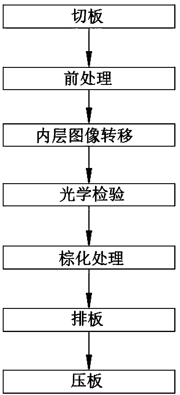
[0023] see figure 1 , the invention provides a technical solution: a manufacturing process for the inner layer of a circuit board, comprising the following steps:

[0024] S1. Cutting board: Cut a large piece of material into the required production size according to the size requirements of different boards, round the corners of the board, clean the dust on the cutting board, remove the glue trace on the board, and remove the board through baking Moisture ab...


PUM


Abstract

The invention discloses a circuit-board internal layer making technology. The technology comprises the following steps of S1, cutting a plate: setting a plate corner to be a round corner, cleaning cutting plate dust, removing a glue mark on the plate, and removing moisture absorbed by a sheet during storage through glazing; S2, carrying out pre-processing; S3, carrying out internal layer image transferring: firstly, uniformly attaching photosensitive ink to a copper surface and carrying out coating processing, then, using ultraviolet light energy to harden a selective local bridge frame, and then, using sodium carbonate to dissolve and wash the ink which is not exposed, leaving a photosensitive portion, carrying out etching to etch away the copper surface of an unexposed exposed-copper portion, and finally, removing a film protecting a line copper surface by sodium oxide with a higher concentration; S4, carrying out optical inspection; S5, carrying out brown processing: cleaning the copper surface through acid pickling, removing the oily substance of the copper surface, providing adaptive preprocessing for mitigating a strengthening drug before browning through preimpregnation, and finally, drying a copper plate surface; S6, typesetting; and S7, pressing the plate.

Description

technical field [0001] The invention relates to the technical field of circuit board manufacturing technology, in particular to a circuit board inner layer manufacturing process. Background technique [0002] Circuit boards include: circuit boards, PCB boards, aluminum substrates, high-frequency boards, PCBs, ultra-thin circuit boards, ultra-thin circuit boards, printed (copper etching technology circuit boards, etc. The circuit board makes the circuit miniaturized and intuitive, for The mass production of fixed circuits and the optimization of the layout of electrical appliances play an important role. In the process of making circuit boards, the inner layer needs to be made. [0003] The current production process of the inner layer of the circuit board has the problems of easy scratching quality, easy oxidation of the copper surface, poor image transfer effect of the inner layer, poor inspection effect and poor adhesion of the copper surface treatment. Contents of the i...

Claims


Application Information

Patent Timeline
Patent Type & Authority Applications(China)
IPC IPC(8): H05K3/46H05K3/00
CPCH05K3/4611H05K3/0085H05K3/4638H05K2203/163H05K2203/166
Inventor 沈利明
Owner 南浔双林荣丰磁材厂
Why Eureka
Try Eureka